CY7C1334 查看數據表(PDF) - Cypress Semiconductor
零件编号
产品描述 (功能)
生产厂家
CY7C1334 Datasheet PDF : 12 Pages
| |||
CY7C1334
Electrical Characteristics Over the Operating Range
Parameter
Description
Test Conditions
Min.
Max.
Unit
VDD
VDDQ
VOH
VOL
VIH
VIL
IX
Power Supply Voltage
I/O Supply Voltage
Output HIGH Voltage
Output LOW Voltage
Input HIGH Voltage
Input LOW Voltage[10]
VDD = Min., IOH = −4.0 mA[12]
VDD = Min., IOL = 8.0 mA[12]
Input Load Current
GND ≤ VI ≤ VDDQ
Input Current of MODE
3.135 3.465
V
3.135 3.465
V
2.4
V
0.4
V
2.0 VDD + 0.3V V
−0.3
0.8
V
−5
5
µA
−30
30
µA
IOZ
Output Leakage
GND ≤ VI ≤ VDDQ, Output Disabled
Current
−5
5
µA
ICC
VDD Operating Supply VDD = Max., IOUT = 0 mA,
7.5-ns cycle, 133 MHz
f = fMAX = 1/tCYC
10-ns cycle, 100 MHz
400
mA
360
mA
12.5-ns cycle, 80 MHz
310
mA
20.0-ns cycle, 50 MHz
260
mA
ISB1
Automatic CE
Max. VDD, Device Deselected, 7.5-ns cycle, 133 MHz
Power-Down
Current-TTL Inputs
VIN ≥ VIH or VIN ≤ VIL
f = fMAX = 1/tCYC
10-ns cycle, 100 MHz
12.5-ns cycle, 80 MHz
60
mA
50
mA
40
mA
20.0-ns cycle, 50 MHz
35
mA
ISB2
Automatic CE
Max. VDD, Device Deselected, All speed grades
Power-Down
VIN ≤ 0.3V or VIN > VDDQ – 0.3V,
Current-CMOS Inputs f = 0
5.0
mA
ISB3
Automatic CE
Max. VDD, Device Deselected, or 7.5-ns cycle, 133 MHz
Power-Down
Current-CMOS Inputs
VIN ≤ 0.3V or VIN > VDDQ – 0.3V
f = fMAX = 1/tCYC
10-ns cycle, 100 MHz
12.5-ns cycle, 80 MHz
50
mA
40
mA
30
mA
20-ns cycle, 50 MHz
25
mA
Capacitance[13]
Parameter
CIN
CCLK
CI/O
Description
Input Capacitance
Clock Input Capacitance
Input/Output Capacitance
Test Conditions
TA = 25°C, f = 1 MHz,
VDD = 3.3V. VDDQ = 3.3V
Max.
4
4
4
Unit
pF
pF
pF
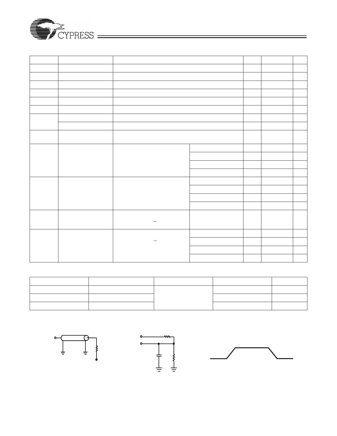
AC Test Loads and Waveforms
OUTPUT
Z0 =50Ω
3.3V
OUTPUT
RL =50Ω
5 pF
R=317Ω
R=351Ω GND
[14]
ALL INPUT PULSES
3.0V
VL = 1.5V
INCLUDING
JIG AND
(a)
SCOPE (b)
1334-2
Notes:
12. The load used for VOH and VOL testing is shown in figure (b) of the A/C test conditions.
13. Tested initially and after any design or process change that may affect these parameters.
14. A/C test conditions assume signal transition time of 2 ns or less, timing reference levels of 1.5V, input pulse levels of 0 to 3.0V, and output loading shown in (a)
of AC Test Loads.
Document #: 38-05065 Rev. **
Page 7 of 12
Share Link: 