MX7534 查看數據表(PDF) - Maxim Integrated
零件编号
产品描述 (功能)
生产厂家
MX7534 Datasheet PDF : 16 Pages
| |||
Microprocessor-Compatible,
14-Bit DACs
VDD
R3
100Ω
R4
33Ω
1 19 2
REF VDD RFB
3
IOUT
VIN
MX7534
AGNDS
4
AGNDF
D7–D0 DGND VSS
5
7–14
6 20
C1
33pF
A1
+
A2
+
INPUT
DATA
NOTE: CONTROL INPUTS OMITTED FOR CLARITY.
RL VO
SIGNAL
GROUND
VDD
R2
10Ω
R1
20Ω 2 1 26 3
REFF REFS VDD RFB
VOLTAGE
REFERENCE
4
IOUT
MX7535 AGNDS
AGNDF 5
D13–D0 DGND VSS 6
8–21
7 27
INPUT
DATA
NOTE: CONTROL INPUTS OMITTED FOR CLARITY.
C1
33pF
A1
+
A2
+
ANALOG
GROUND
RL VO
SIGNAL
GROUND
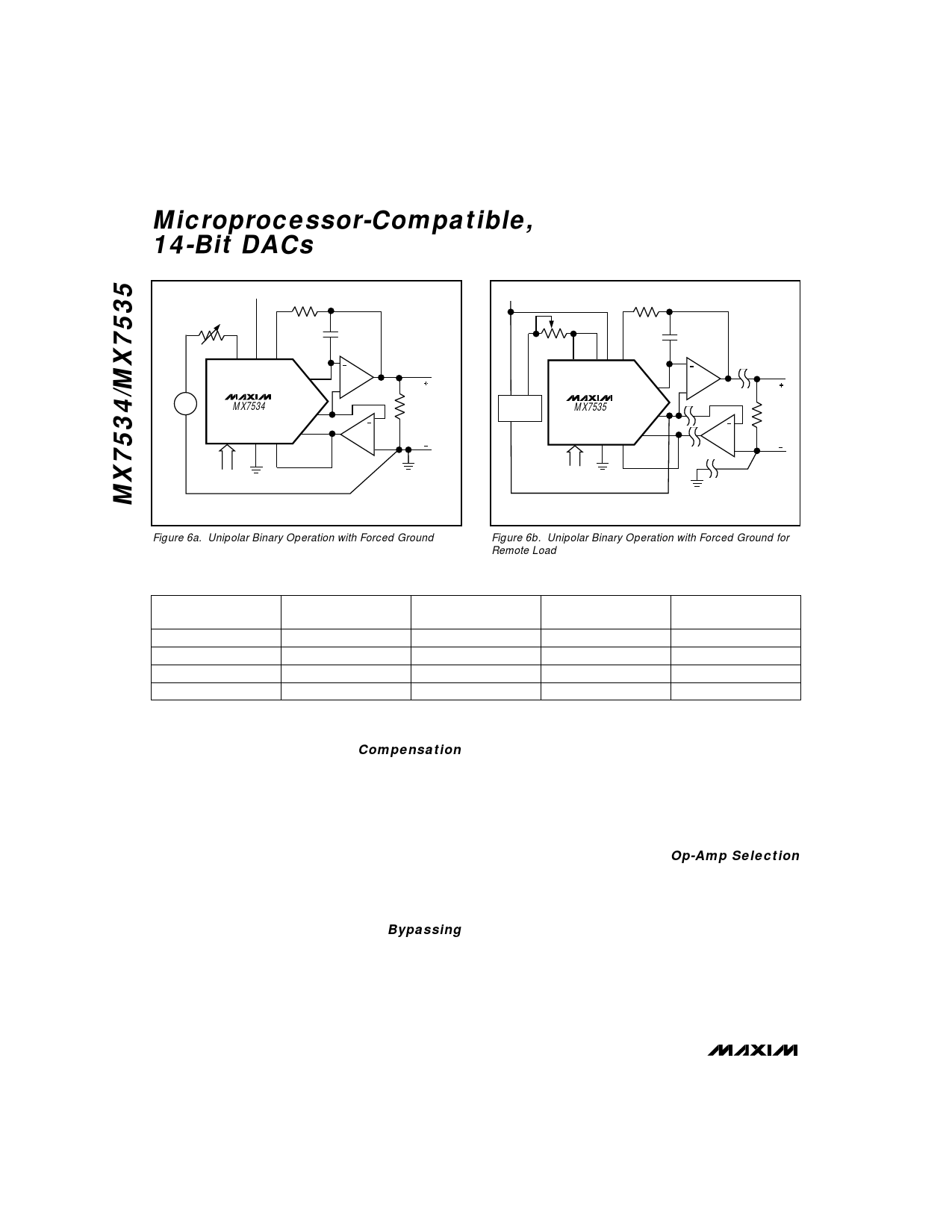
Figure 6a. Unipolar Binary Operation with Forced Ground
Figure 6b. Unipolar Binary Operation with Forced Ground for
Remote Load
Table 5. Amplifier Performance Comparisons
OP AMP
MAX400
Maxim OP07
AD554L*
HA2620*
INPUT OFFSET
VOLTAGE (VOS)
10µV
25µV
500µV
4mV
INPUT BIAS
CURRENT (IB)
2nA
2nA
25pA
35nA
* AD544L is an Analog Devices part; HA2620 is a Harris Semiconductor part.
OFFSET VOLTAGE
DRIFT (TC VOS)
0.3µV/°C
0.6µV/°C
5µV/°C
20µV/°C
SETTLING
TO 0.003% FS
50µs
50µs
5µs
0.8µs
Compensation
A compensation capacitor, C1, may be needed when
the DAC is used with a high-speed output amplifier.
The capacitor cancels the pole formed by the DAC’s
output capacitance and internal feedback resistance.
Its value depends on the type of op amp used, but typi-
cal values range from 10pF to 33pF. Too small a value
causes output ringing, while excess capacitance over-
damps the output. Minimize C1’s size and improve out-
put settling performance by keeping the PC board
trace as short as possible and stray capacitance at
IOUT as small as possible.
Bypassing
Place a 1µF bypass capacitor, in parallel with a 0.01µF
ceramic capacitor, as close to the DAC’s VDD and GND
pins as possible. Use a 1µF tantalum bypass capacitor
to optimize high-frequency noise rejection. Place a
4.7µF decoupling capacitor at VSS to minimize the DAC
output leakage current.
The MX7534/MX7535 have high-impedance digital
inputs. To minimize noise pickup, connect them to
either VDD or GND terminals when not in use. Connect
active inputs to VDD or GND through high-value resis-
tors (1MΩ) to prevent static charge accumulation if
these pins are left floating, as might be the case when
a circuit card is left unconnected.
Op-Amp Selection
Input offset voltage (VOS), input bias current (IB), and
offset voltage drift (TC VOS) are three key parameters in
determining the choice of a suitable amplifier. To main-
tain specified accuracy with VREF of 10V, VOS should
be less than 30µV and IB should be less than 2nA.
Open-loop gain should be greater than 340,000.
Maxim’s MAX400 has low VOS (10µV max), low IB
(2nA), and low TC VOS (0.3µV/°C max). This op amp
can be used without requiring any adjustments. For
10 ______________________________________________________________________________________
Share Link: 