NB3N502DG 查看數據表(PDF) - ON Semiconductor
零件编号
产品描述 (功能)
生产厂家
NB3N502DG Datasheet PDF : 5 Pages
| |||
NB3N502
14 MHz to 190 MHz PLL
Clock Multiplier
Description
The NB3N502 is a clock multiplier device that generates a low jitter,
TTL/CMOS level output clock which is a precise multiple of the
external input reference clock signal source. The device is a cost
efficient replacement for the crystal oscillators commonly used in
electronic systems. It accepts a standard fundamental mode crystal or
an external reference clock signal. Phase−Locked−Loop (PLL) design
techniques are used to produce an output clock up to 190 MHz with a
50% duty cycle. The NB3N502 can be programmed via two select
inputs (S0, S1) to provide an output clock (CLKOUT) at one of six
different multiples of the input frequency source, and at the same time
output the input aligned reference clock signal (REF).
Features
• Clock Output Frequency up to 190 MHz
• Operating Range: VDD = 3 V to 5.5 V
• Low Jitter Output of 15 ps One Sigma (rms)
• Zero ppm Clock Multiplication Error
• 45% − 55% Duty Cycle
• 25 mA TTL−level Drive Outputs
• Crystal Reference Input Range of 5 − 27 MHz
• Input Clock Frequency Range of 2 − 50 MHz
• Available in 8−pin SOIC Package or in Die Form
• Full Industrial Temperature Range −40°C to 85°C
• This is a Pb−Free Device
VDD
http://onsemi.com
8
1
SOIC−8
D SUFFIX
CASE 751
MARKING DIAGRAM
8
3N502
ALYW
G
1
3N502 = Specific Device Code
A
= Assembly Location
L
= Wafer Lot
Y
= Year
W
= Work Week
G
= Pb−Free Package
ORDERING INFORMATION
Device
Package
Shipping†
NB3N502DG
SOIC−8
(Pb−Free)
98 Units/Rail
NB3N502DR2G SOIC−8 2500/Tape & Reel
(Pb−Free)
†For information on tape and reel specifications,
including part orientation and tape sizes, please
refer to our Tape and Reel Packaging Specification
Brochure, BRD8011/D.
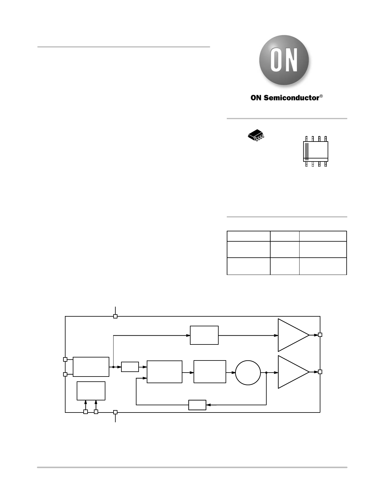
X1/CLK
X2
Reference
Clock
Crystal
Oscillator
÷P
Multiplier
Select
S1 S0
GND
Phase
Detector
Charge
Pump
VCO
Feedback
÷M
Figure 1. NB3N502 Logic Diagram
TTL/
CMOS
Output
TTL/
CMOS
Output
REF
CLKOUT
© Semiconductor Components Industries, LLC, 2006
1
March, 2006 − Rev. 0
Publication Order Number:
NB3N502/D
Share Link: 