NB3N508SDTG 查看數據表(PDF) - ON Semiconductor
零件编号
产品描述 (功能)
生产厂家
NB3N508SDTG Datasheet PDF : 8 Pages
| |||
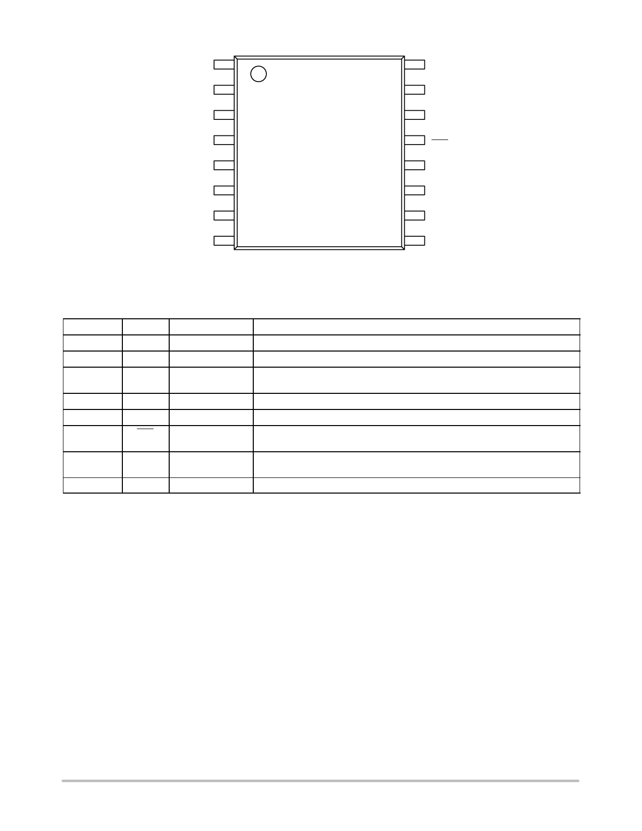
NB3N508S
X1 1
16 X2
VDD 2
15 NC
VDD 3
14 CLK
VDD 4
VIN 5
NB3N508S
13 CLK
12 GND
GND 6
11 NC
GND 7
10 VDD
GND 8
9 NC
Figure 2. Pin Configuration (Top View)
Table 1. PIN DESCRIPTION
Pin
Name
I/O
1
X1
Crystal Input
2, 3, 4, 10
VDD
5
VIN
Power Supply
Input
6, 7, 8, 12
9, 11, 15
13
GND
NC
CLK
Power Supply
−
M−LVDS Output
14
CLK
M−LVDS Output
16
X2
Crystal Input
Description
Crystal input(IN). Connect to a 27 MHz crystal.
Positive power supply voltage.
Analog voltage input pin that controls output oscillation frequencies. VIN pin range is
from 0 V to 3.3 V. VIN voltage should not exceed VDD.
Ground 0 V. These pins provide GND return path for the devices.
No Connect.
Inverted clock output. Typically loaded with 50 W receiver termination resistor across
diff. pair.
Noninverted clock output. Typically loaded with 50 W receiver termination resistor
across diff. pair.
Crystal input(OUT). Connect to a 27 MHz crystal.
Recommended Crystal Parameters
Crystal Fundamental AT−Cut Frequency
Load Capacitance
Shunt Capacitance, C0
Max Equivalent Series Resistance
Max Initial Accuracy at 25°C
Temperature Stability
Aging
C0/C1 Ration
27 MHz
14 pF
7 pF
35 W
±20 ppm
±30 ppm
±20 ppm
250 Max
http://onsemi.com
3
Share Link: 