NCP1072STBT3G(2012) 查看數據表(PDF) - ON Semiconductor
零件编号
产品描述 (功能)
生产厂家
NCP1072STBT3G Datasheet PDF : 26 Pages
| |||
NCP1072, NCP1075
MAXIMUM RATINGS TABLE
Symbol
Rating
Value
Unit
VCC
BVdss
Power Supply Voltage on all pins, except Pin 5(Drain)
Drain voltage
−0.3 to 10
V
−0.3 to 700
V
IDS(PK)
I_VCC
RqJ−A
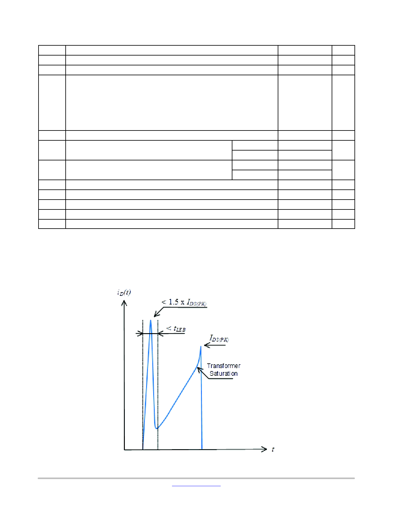
Drain Current Peak during Transformer Saturation
Maximum Current into Pin 1 when Activating the 8.2 V Active Clamp
P Suffix, Case 626A
Junction−to−Air, 2.0 oz Printed Circuit Copper Clad
0.36 Sq. Inch
1.0 Sq. Inch
2 x IIpeak(0)
15
77
60
A
mA
°C/W
RqJ−A
ST Suffix, Plastic Package Case 318E
Junction−to−Air, 2.0 oz Printed Circuit Copper Clad
0.36 Sq. Inch
1.0 Sq. Inch
74
°C/W
55
TJMAX
Maximum Junction Temperature
Storage Temperature Range
150
°C
−60 to +150
°C
ESD Capability, HBM model (All pins except HV)
2
kV
ESD Capability, Machine Model
200
V
Stresses exceeding Maximum Ratings may damage the device. Maximum Ratings are stress ratings only. Functional operation above the
Recommended Operating Conditions is not implied. Extended exposure to stresses above the Recommended Operating Conditions may affect
device reliability.
1. This device series contains ESD protection and exceeds the following tests:
Human Body Model 2000 V per JEDEC JESD22−A114−F
Machine Model Method 200 V per JEDEC JESD22−A115−A
2. This device contains latch−up protection and exceeds 100 mA per JEDEC Standard JESD78
ELECTRICAL CHARACTERISTICS
(For typical values TJ = 25°C, for min/max values TJ = −40°C to +125°C, VCC = 8 V unless otherwise noted)
Symbol
Rating
Pin
Min
Typ
Max
Unit
SUPPLY SECTION AND VCC MANAGEMENT
VCC(on) VCC increasing level at which the switcher starts operation
VCC(min) VCC decreasing level at which the HV current source restarts
VCC(off) VCC decreasing level at which the switcher stops operation (UVLO)
VCC(reset) VCC voltage at which the internal latch is reset (guaranteed by design)
VCC(clamp) Offset voltage above VCC(on) at which the internal clamp activates
ICC1
Internal IC consumption, MOSFET switching at 65 kHz
ICCskip Internal IC consumption, FB is 0 V (No switching on MOSFET)
POWER SWITCH CIRCUIT
1
7.8
8.2
8.6
V
1
6.5
6.8
7.2
V
1
6.1
6.3
6.6
V
1
4
V
1
130
190
300
mV
1
0.7
1.0
mA
1
360
mA
RDS(on)
BVDSS
IDSS(off)
Power Switch Circuit on−state resistance
NCP107x (Id = 50 mA)
TJ = 25°C
TJ = 125°C
Power Switch Circuit & Startup breakdown voltage
(ID(off) = 120 mA, TJ = 25°C)
Power Switch & Startup breakdown voltage off−state leakage current
TJ = 125°C (Vds = 700 V)
5
W
11
16
19
24
5
700
V
mA
5
85
Switching characteristics (RL=50 W, VDS set for Idrain = 0.7 x Ilim)
ton
Turn−on time (90% − 10%)
5
toff
Turn−off time (10% − 90%)
5
ns
20
10
INTERNAL START−UP CURRENT SOURCE
Istart1
High−voltage current source, VCC = VCC(on) – 200 mV
5
5
9
12
mA
3. The final switch current is: IIPK(0) / (Vin/LP + Sa) x Vin/LP + Vin/LP x tprop, with Sa the built−in slope compensation, Vin the input voltage, LP
the primary inductor in a flyback, and tprop the propagation delay..
4. NCP1072 130 kHz on demand only.
5. Oscillator frequency is measured with disabled jittering.
http://onsemi.com
4
Share Link: 