NCP1601A 查看數據表(PDF) - ON Semiconductor
零件编号
产品描述 (功能)
生产厂家
NCP1601A Datasheet PDF : 18 Pages
| |||
NCP1601A, NCP1601B
be too bulky because it can pollute the power factor by
distorting the rectified sinusoidal input voltage.
Iin
Vin
IL
L
Vout
Cfilter
Cbulk
Power factor is corrected when the input impedance Zin
in (eq.3) are constant or slowly varying.
The MOSFET on time t1 or PFC modulation duty is
generated by a feedback signal Vton and a ramp. The PFC
modulation circuit and timing diagram are shown in
Figure 28. A relationship in (eq.4) is obtained.
t1
+
Cramp Vton
Ich
(eq.4)
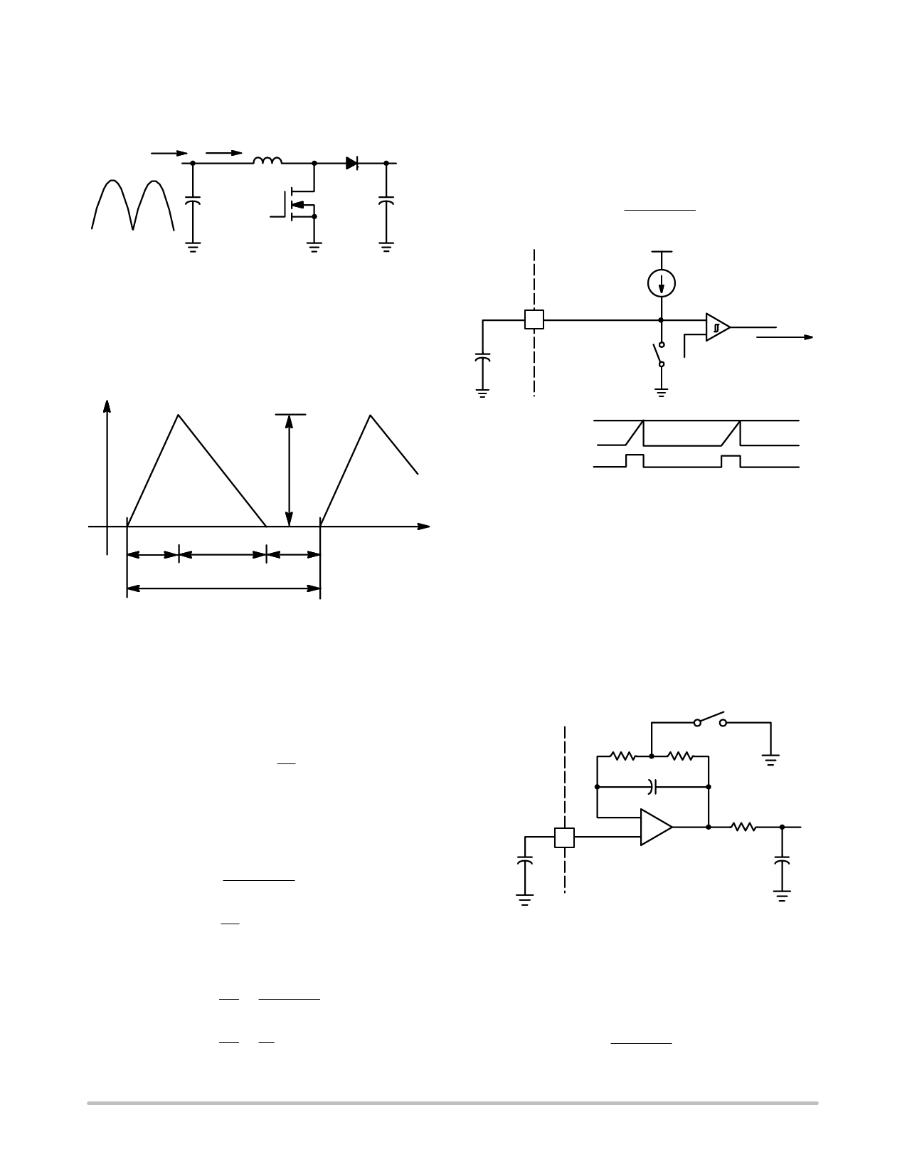
Figure 26. DCM/CRM PFC Boost Converter
PFC Methodology
NCP1601 uses a proprietary PFC methodology
particularly designed for both DCM and CRM operation.
The PFC methodology is described in this section.
Inductor Current
Ipk
t1
t2
t3
T
time
Figure 27. Inductor Current in DCM
As shown in Figure 27, the inductor current IL of each
switching cycle starts from zero in DCM. CRM is a special
case of DCM when t3 = 0. When the PFC boost converter
MOSFET is on, the inductor current IL increases from zero
to Ipk for a time duration t1 with inductance L and input
voltage Vin. (eq.1) is formulated.
Vin
+
L
Ipk
t1
(eq.1)
The input filter capacitor Cfilter and the front−ended EMI
filter absorb the high−frequency component of inductor
current. It makes the input current Iin a low−frequency
signal.
Iin
+
Ipk
(t1 )
2T
t2)
for DCM (eq.2a)
Iin
+
Ipk
2
for CRM (eq.2b)
From (eq.1) and (eq.2), the input impedance Zin is
formulated.
Zin
+
Vin
Iin
+
2TL
t1(t1 )
t2)
for DCM
(eq.3a)
Zin
+
Vin
Iin
+
2L
t1
for CRM (eq.3b)
Ramp
3
Cramp
Ich
closed when
output low
PFC
Modulation
+
−
Vton
Turns off
MOSFET
Vton
ramp
output
Figure 28. PFC Modulation Circuit and Timing
Diagram
The charging current Ich is constant 100 mA current and
the ramp capacitor Cramp is constant for a particular design.
Hence, according to (eq.4) the MOSFET on time t1 is
proportional to Vton.
In order to protect the PFC modulation comparator, the
maximum voltage of Vton is limited to internal clamp
Vton(max) (3.9 V typical) and the ramp pin (Pin 3) is with a
9 V ESD Zener diode. The 3.9 V maximum limit of this
Vton indirectly limits the maximum on time.
closed when zero current
R1
R2
Vcontrol
2
Ccontrol
C1
−
+
R3
Vton
C3
Figure 29. Vcontrol Processing Circuit
The Vcontrol processing circuit generates Vton from
control voltage Vcontrol and time information of zero
inductor current. The circuit in Figure 29 makes (eq.5)
where the value of resistor R1 is much higher than the value
of resistor R2 (R1 >> R2).
Vton
+
T
Vcontrol
t1 ) t2
for DCM (eq.5a)
http://onsemi.com
10
Share Link: 