NCP3065 查看數據表(PDF) - ON Semiconductor
零件编号
产品描述 (功能)
生产厂家
NCP3065 Datasheet PDF : 18 Pages
| |||
NCP3065, NCV3065
INTRODUCTION
The NCP3065 is a monolithic power switching regulator
optimized for LED Driver applications. Its flexible
architecture enables the system designer to directly
implement a step-up or step-down topology with a
minimum number of external components for driving LEDs.
A representative block diagram is shown in Figure 4.
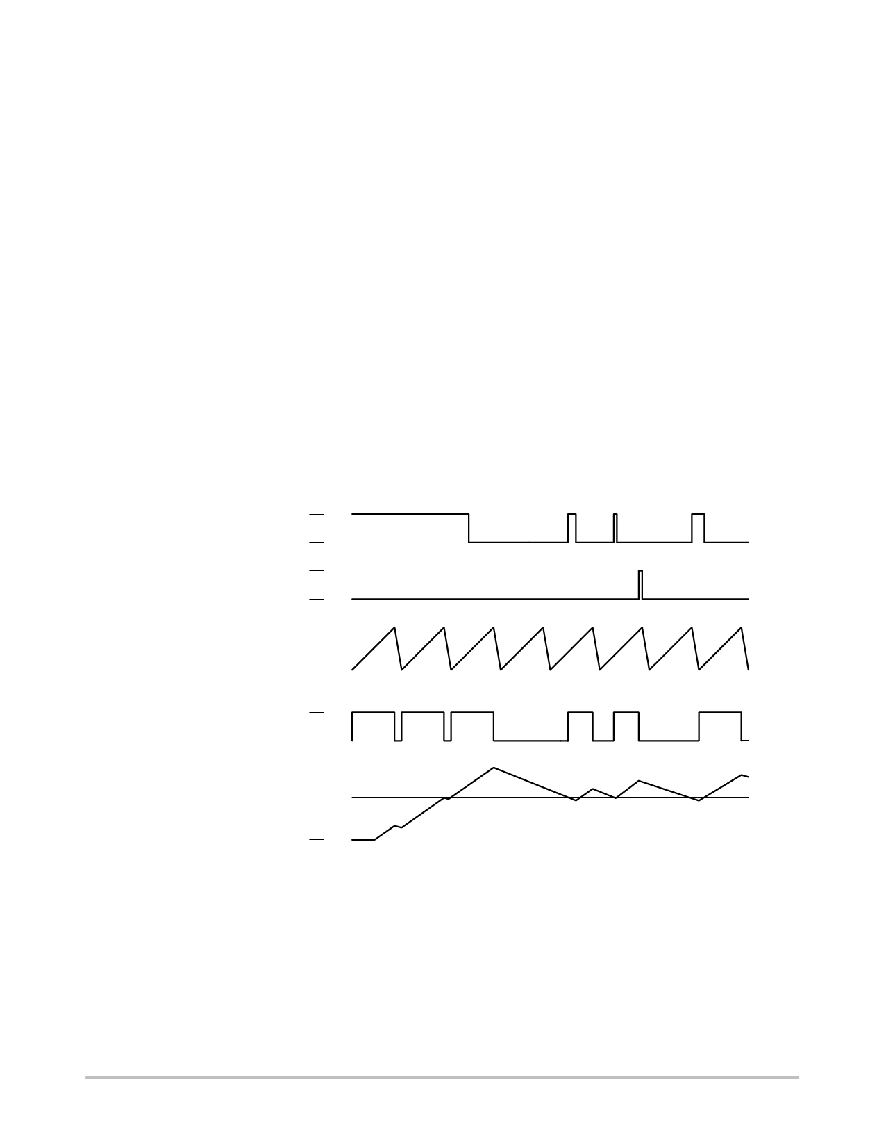
OPERATING DESCRIPTION
The NCP3065 operates as a fixed oscillator frequency
output voltage ripple gated regulator. In general, this mode
of operation is somewhat analogous to a capacitor charge
pump and does not require dominant pole loop
compensation for converter stability. The typical operating
waveforms are shown in Figure 14. The output voltage
waveform shown is for a step-down converter with the
ripple and phasing exaggerated for clarity. During initial
converter startup, the feedback comparator senses that the
output voltage level is below nominal. This causes the
output switch to turn on and off at a frequency and duty cycle
controlled by the oscillator, thus pumping up the output filter
capacitor. When the feedback voltage level reaches nominal
comparator value, the output switch cycle is inhibited. When
the load current causes the output voltage to fall below the
nominal value feedback comparator enables switching
immediately. Under these conditions, the output switch
conduction can be enabled for a partial oscillator cycle, a
partial cycle plus a complete cycle, multiple cycles, or a
partial cycle plus multiple cycles.
Oscillator
The oscillator frequency and off-time of the output switch
are programmed by the value of the timing capacitor CT.
Capacitor CT is charged and discharged by a 1 to 6 ratio
internal current source and sink, generating a positive going
sawtooth waveform at Pin 3. This ratio sets the maximum
tON/(tON+tOFF) of the switching converter as 6/(6+1) or
85.7% (typical). The oscillator peak and valley voltage
difference is 500 mV typically. To calculate the CT capacitor
value for required oscillator frequency, use the equations
found in Figure 22. An online NCP3065 design tool can be
found at www.onsemi.com, which adds in selecting
component values.
1
Feedback Comparator Output
0
1
IPK Comparator Output
0
Timing Capacitor, CT
On
Output Switch
Off
Nominal Output Voltage Level
Output Voltage
Startup
Operation
Figure 14. Typical Operating Waveforms
http://onsemi.com
7
Share Link: 