NCP5608 查看數據表(PDF) - ON Semiconductor
零件编号
产品描述 (功能)
生产厂家
NCP5608 Datasheet PDF : 16 Pages
| |||
NCP5608
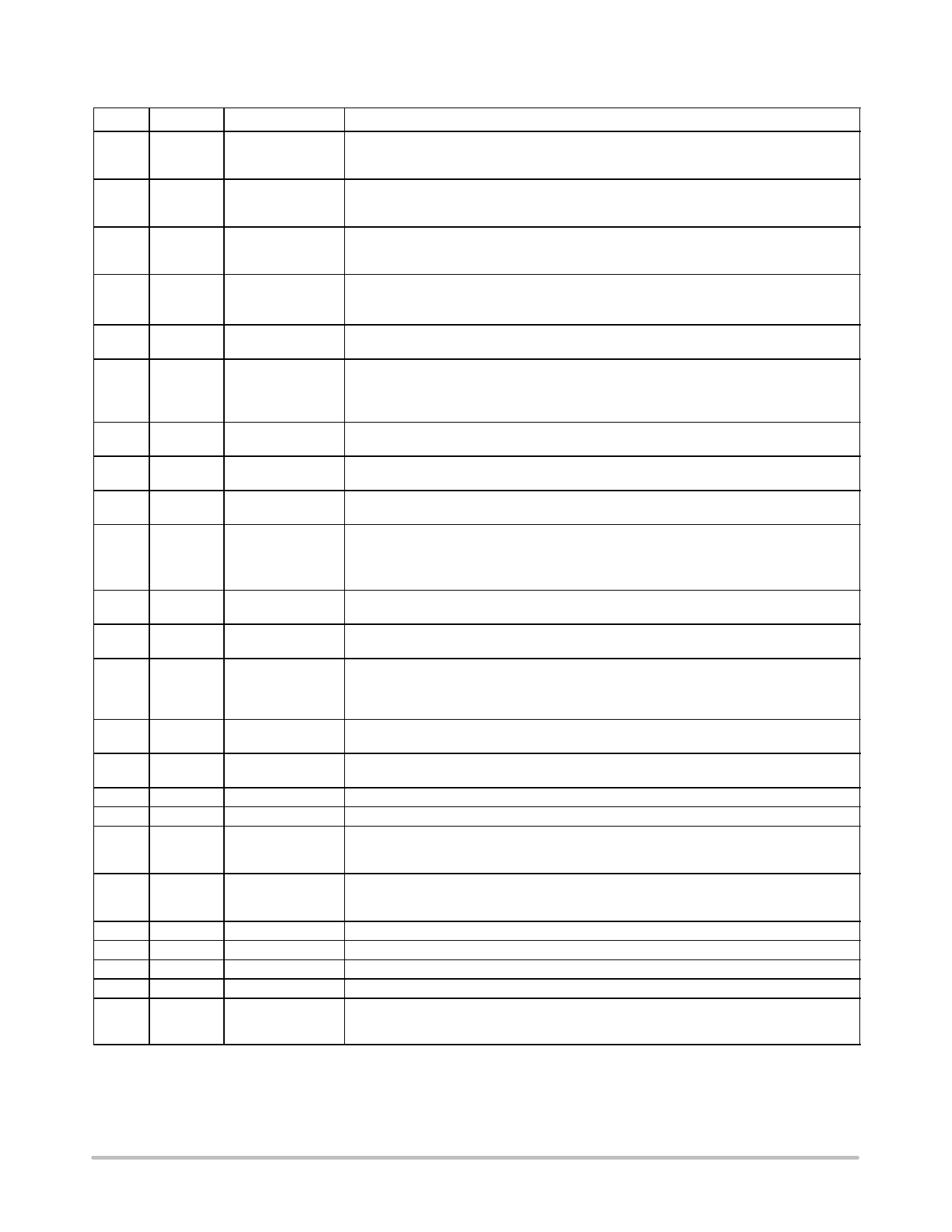
PIN FUNCTION DESCRIPTION
Pin
Symbol
Type
Description
1
AGND
GROUND
This pin is the NCP5608 analog ground and shall be connected to the system ground. Care
must be observed to minimize the total parasitic inductance between the pin and the ground
plane.
2
IREFFL OUTPUT, ANALOG This pin is used to set up the current reference for the FLASH output currents (LED5 to
LED8). The reference current is derived from the internal bandgap voltage to ground by
means of an external resistor. (Note 1)
3
IREFBK OUTPUT, ANALOG This pin is used to set up the current reference for the BACK LIGHT output currents (LED1
to LED4). The reference current is derived from the internal bandgap voltage to ground by
means of an external resistor. (Note 1)
4
SDA
INPUT, DIGITAL This pin, associated with the SCL signal, carries the DATA signal to set up the selected
output LED current.
The DATA signal is built with a single SDA line to support the I2C protocol.
5
SCL
INPUT, DIGITAL This is the clock signal associated with the SDA pins. The pin carries the standard CLOCK
signal to operate the I2C protocol.
6
CCMP ANALOG, INPUT This pin is connected to the internal I2C bias network and must be either left open, or
bypassed to ground by a 10 nF ceramic capacitor when the I2C voltage drops below 1.8 V.
Such a capacitor compensate the voltage drop during normal operation, keeping in mind it is
not mandatory when the I2C voltage is 1.8 V and above.
7
LED1
INPUT, POWER This pin sinks to ground the current flowing into the first LED, and is intended to be used in
backlight application. The current is limited to 30 mA max. (Note 2)
8
LED2
INPUT, POWER This pin sinks to ground the current flowing into the second LED, and is intended to be used
in backlight application. The current is limited to 30 mA max. (Note 2)
9
LED3
INPUT, POWER This pin sinks to ground the current flowing into the third LED, and is intended to be used in
backlight application. The current is limited to 30 mA max. (Note 2)
10
LED4
INPUT, POWER This pin sinks to ground the current flowing into the fourth LED, and is intended to be used
in backlight application. The current is limited to 30 mA max. (Note 2)
On the other hand, LED4 can be disconnected when only three LEDs are used in the
backlight application. (Table 1)
11
LED5
INPUT, POWER This pin sinks to ground the current flowing into the fifth LED (100 mA max), and is intended
to be used in Flash application. (Note 2)
12
LED6
INPUT, POWER This pin sinks to ground the current flowing into the sixth LED (100 mA max), and is
intended to be used in Flash or high power application. (Note 2)
13 PWRGND
POWER
This pin provides the ground reference for the power elements and must be connected to
the system ground by a heavy track. Using the ground plane technique is strongly
recommended. Care must be observed to minimize the total parasitic inductance between
the pin and the ground plane.
14
LED7
INPUT, POWER This pin sinks to ground the current flowing into the seventh LED (100 mA max), and is
intended to be used in flash or high power application. (Note 2)
15
LED8
INPUT, POWER This pin sinks to ground the current flowing into the eighth LED (100 mA max), and is
intended to be used in flash or high power application. (Note 2)
16
C1N
POWER
This pin is the second side of the C1 fly capacitor.
17
C1P
POWER
This pin is the first side of the C1 fly capacitor.
18
VOUT OUTPUT, POWER This pin provides the output power to the external LED. Since the regulation is based on a
current loop, the voltage will varies as the output current varies in the application. The Vout
pin must be bypassed to GND by a 4.7 mF ceramic capacitor. (Note 3)
19
PVBAT
INPUT, POWER This pin provides the supply voltage to the charge pump converter. The pin must be
connected to the AVbat supply source and bypassed to GND by a 10 mF/16 V ceramic
capacitor. (Note 3) Using a power plane is recommended.
20
C2N
POWER
This pin is the second side of the C2 fly capacitor.
21
C2P
POWER
This pin is the first side of the C2 fly capacitor.
22
C3P
POWER
This pin is the second side of the C3 fly capacitor.
23
C3N
POWER
This pin is the first side of the C3 fly capacitor.
24
AVbat
INPUT, POWER This pin provides the supply voltage to the analog and digitals blocks. The pin must be
connected to the PVbat supply source and bypassed to GND by a 1 mF/16 V ceramic
capacitor. (Note 3) Using a power plane is recommended.
1. To achieve a good accuracy of the LED current, 1% tolerance resistor, with 100 ppm stability, or better, shall be used. The reference current
is internally mirrored and sized according to the programmed value for a given external LED.
2. Total DC−DC output current is limited to 500 mA.
3. Ceramic X7R, ESR < 50 mW ESL < 0.5 nH, SMD types capacitors are mandatory to achieve the Iout specifications. On the other hand, care
must be observed to take into account the DC bias impact on the capacitance value; see ceramic capacitor manufacturer data sheets.
http://onsemi.com
4
Share Link: 