NCV47701 查看數據表(PDF) - ON Semiconductor
零件编号
产品描述 (功能)
生产厂家
NCV47701 Datasheet PDF : 14 Pages
| |||
NCV47701
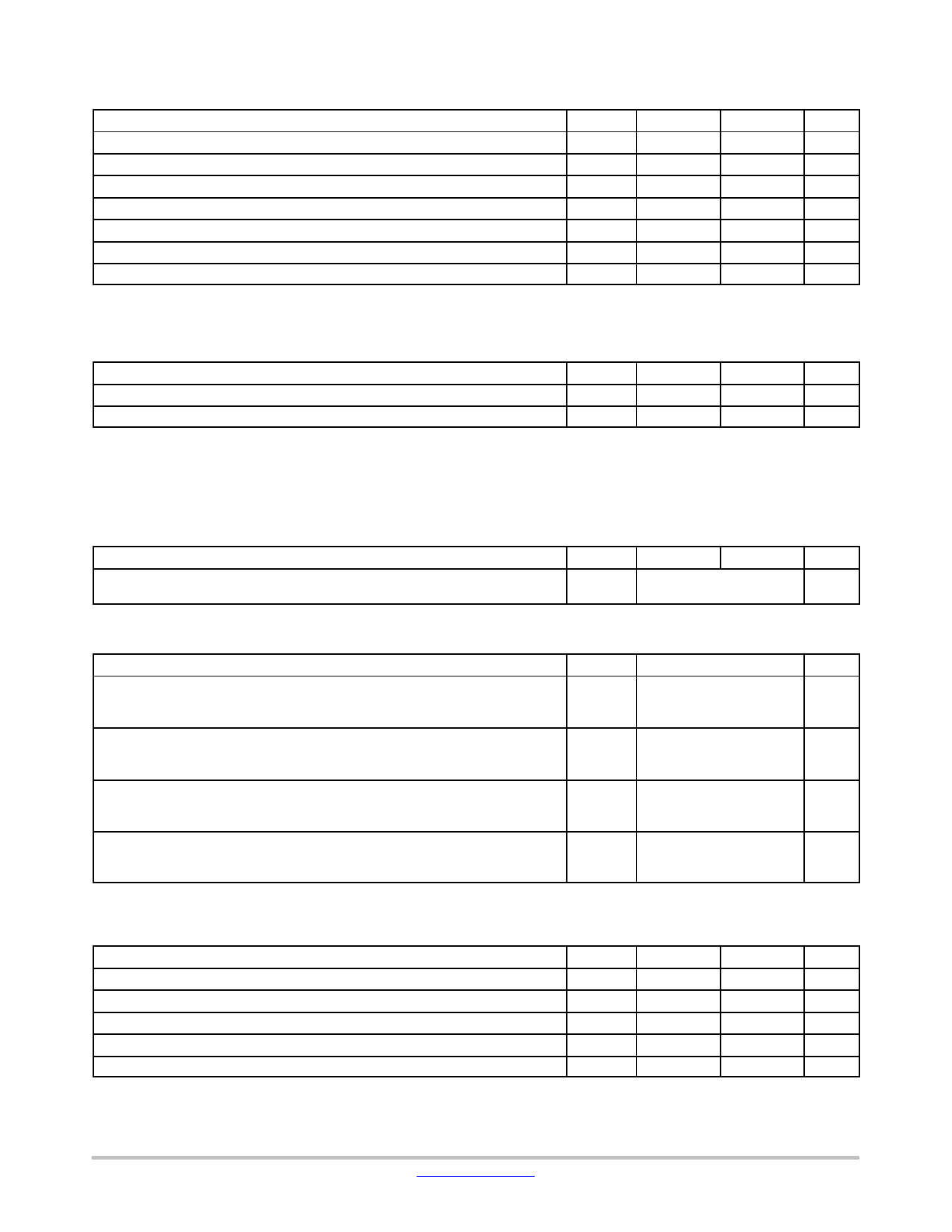
ABSOLUTE MAXIMUM RATINGS (Note 1)
Rating
Symbol
Min
Max
Unit
Input Voltage
Vin
−42
45
V
Enable Input Voltage
VEN
−42
45
V
Adjustable Input Voltage
VADJ
−0.3
10
V
CSO Voltage
VCSO
−0.3
7
V
Output Voltage
Vout
−1
40
V
Junction Temperature
TJ
−40
150
°C
Storage Temperature
TSTG
−55
150
°C
Stresses exceeding those listed in the Maximum Ratings table may damage the device. If any of these limits are exceeded, device functionality
should not be assumed, damage may occur and reliability may be affected.
1. Refer to ELECTRICAL CHARACTERISTICS and APPLICATION INFORMATION for Safe Operating Area.
ESD CAPABILITY (Note 2)
Rating
Symbol
Min
Max
Unit
ESD Capability, Human Body Model
ESDHBM
−2
2
kV
ESD Capability, Machine Model
ESDMM
−200
200
V
2. This device series incorporates ESD protection and is tested by the following methods:
ESD Human Body Model tested per AEC−Q100−002 (JS−001−2010)
ESD Machine Model tested per AEC−Q100−003 (EIA/JESD22−A115)
Field Induced Charge Device Model ESD characterization is not performed on plastic molded packages with body sizes < 50mm2 due to
the inability of a small package body to acquire and retain enough charge to meet the minimum CDM discharge current waveform
characteristic defined in JEDEC JS−002−2014.
LEAD SOLDERING TEMPERATURE AND MSL (Note 3)
Rating
Symbol
Min
Max
Unit
Moisture Sensitivity Level
SOIC−8 EP
MSL
2
−
SOIC−8
1
3. For more information, please refer to our Soldering and Mounting Techniques Reference Manual, SOLDERRM/D
THERMAL CHARACTERISTICS
Rating
Symbol
Value
Unit
Thermal Characteristics, SOIC−8 EP (single layer PCB)
Thermal Resistance, Junction−to−Air (Note 4)
Thermal Reference, Junction−to−Lead (Note 4)
RθJA
RψJL
°C/W
70
19
Thermal Characteristics, SOIC−8 EP (4 layers PCB)
Thermal Resistance, Junction−to−Air (Note 4)
Thermal Reference, Junction−to−Lead (Note 4)
RθJA
RψJL
°C/W
29
12
Thermal Characteristics, SOIC−8 (single layer PCB)
Thermal Resistance, Junction−to−Air (Note 4)
Thermal Reference, Junction−to−Lead (Note 4)
RθJA
RψJL
°C/W
121
42
Thermal Characteristics, SOIC−8 (4 layers PCB)
Thermal Resistance, Junction−to−Air (Note 4)
Thermal Reference, Junction−to−Lead (Note 4)
RθJA
RψJL
°C/W
77
52
4. Values based on copper area of 645 mm2 (or 1 in2) of 1 oz copper thickness and FR4 PCB substrate. Single layer − according to JEDEC51.3,
4 layers − according to JEDEC51.7.
RECOMMENDED OPERATING RANGES
Rating
Symbol
Min
Max
Unit
Input Voltage (Note 5)
Vin
5.5
40
V
Output Current Limit (Note 6)
ILIM
10
350
mA
Junction Temperature
TJ
−40
150
°C
Nominal Output Voltage
Vout_nom
5.0
20
V
Current Sense Output (CSO) Capacitor
CCSO
1.0
4.7
mF
Functional operation above the stresses listed in the Recommended Operating Ranges is not implied. Extended exposure to stresses beyond
the Recommended Operating Ranges limits may affect device reliability.
5. Minimum Vin = 5.5 V or (Vout_nom + 0.5 V), whichever is higher.
6. Corresponding RCSO is in range from 25 kW down to 728 W.
www.onsemi.com
3
Share Link: 