NDS355N 查看數據表(PDF) - Fairchild Semiconductor
零件编号
产品描述 (功能)
生产厂家
NDS355N Datasheet PDF : 7 Pages
| |||
Electrical Characteristics (TA = 25°C unless otherwise noted)
Symbol Parameter
Conditions
Min Typ Max Units
DRAIN-SOURCE DIODE CHARACTERISTICS AND MAXIMUM RATINGS
IS
Maximum Continuous Source Current
0.6
A
ISM
Maximum Pulse Source Current (Note 2)
6
A
VSD
Drain-Source Diode Forward Voltage
VGS = 0 V, IS = 1.6 A
0.8 1.2
V
Notes:
1. RθJA is the sum of the junction-to-case and case-to-ambient thermal resistance where the case thermal reference is defined as the solder mounting surface of the drain pins. RθJC is guaranteed by
design while RθCA is determined by the user's board design.
( ) = = = ( ) × PD t
TJ −TA
RθJ A(t)
TJ −TA
RθJ C+RθCA(t)
I
2
D
t
RDS(ON ) TJ
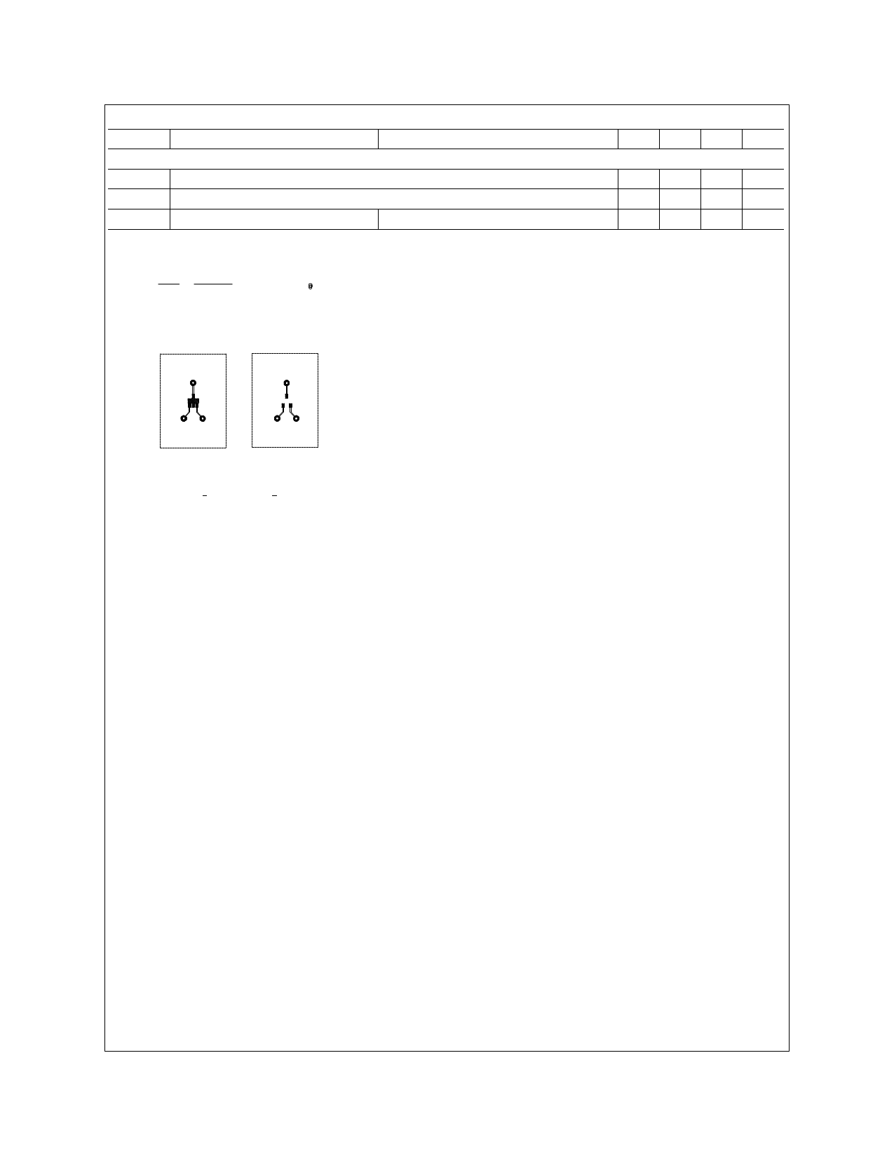
Typical RθJA using the board layouts shown below on 4.5"x5" FR-4 PCB in a still air environment:
a. 250oC/W when mounted on a 0.02 in2 pad of 2oz cpper.
b. 270oC/W when mounted on a 0.001 in2 pad of 2oz cpper.
1a
1b
Scale 1 : 1 on letter size paper
2. Pulse Test: Pulse Width < 300µs, Duty Cycle < 2.0%.
NDS355N Rev. D1
Share Link: 