NDS352AP 查看數據表(PDF) - Fairchild Semiconductor
零件编号
产品描述 (功能)
生产厂家
NDS352AP Datasheet PDF : 6 Pages
| |||
February 1997
NDS352AP
P-Channel Logic Level Enhancement Mode Field Effect Transistor
General Description
These P -Channel logic level enhancement mode power field
effect transistors are produced using Fairchild's proprietary,
high cell density, DMOS technology. This very high density
process is especially tailored to minimize on-state resistance.
These devices are particularly suited for low voltage applications
such as notebook computer power management, portable
electronics, and other battery powered circuits where fast
high-side switching, and low in-line power loss are needed in a
very small outline surface mount package.
Features
-0.9 A, -30 V. RDS(ON) = 0.5 Ω @ VGS = -4.5 V
RDS(ON) = 0.3 Ω @ VGS = -10 V.
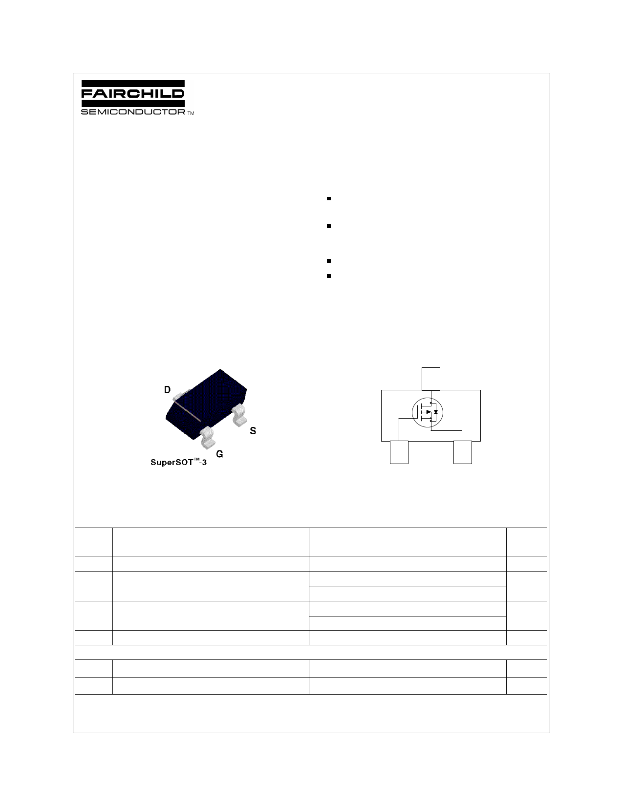
Industry standard outline SOT-23 surface mount package
using proprietary SuperSOTTM-3 design for superior thermal
and electrical capabilities.
High density cell design for extremely low RDS(ON).
Exceptional on-resistance and maximum DC current
capability.
________________________________________________________________________________
D
G
S
Absolute Maximum Ratings
Symbol Parameter
TA = 25°C unless otherwise noted
VDSS
Drain-Source Voltage
VGSS
Gate-Source Voltage - Continuous
ID
Maximum Drain Current - Continuous
- Pulsed
(Note 1a)
PD
Maximum Power Dissipation
(Note 1a)
(Note 1b)
TJ,TSTG Operating and Storage Temperature Range
THERMAL CHARACTERISTICS
RθJA
RθJC
Thermal Resistance, Junction-to-Ambient
Thermal Resistance, Junction-to-Case
(Note 1a)
(Note 1)
© 1997 Fairchild Semiconductor Corporation
NDS352AP
-30
±20
±0.9
±10
0.5
0.46
-55 to 150
250
75
Units
V
V
A
W
°C
°C/W
°C/W
NDS352AP Rev.D
Share Link: 