AD7472BRU(2000) 查看數據表(PDF) - Analog Devices
零件编号
产品描述 (功能)
生产厂家
AD7472BRU Datasheet PDF : 16 Pages
| |||
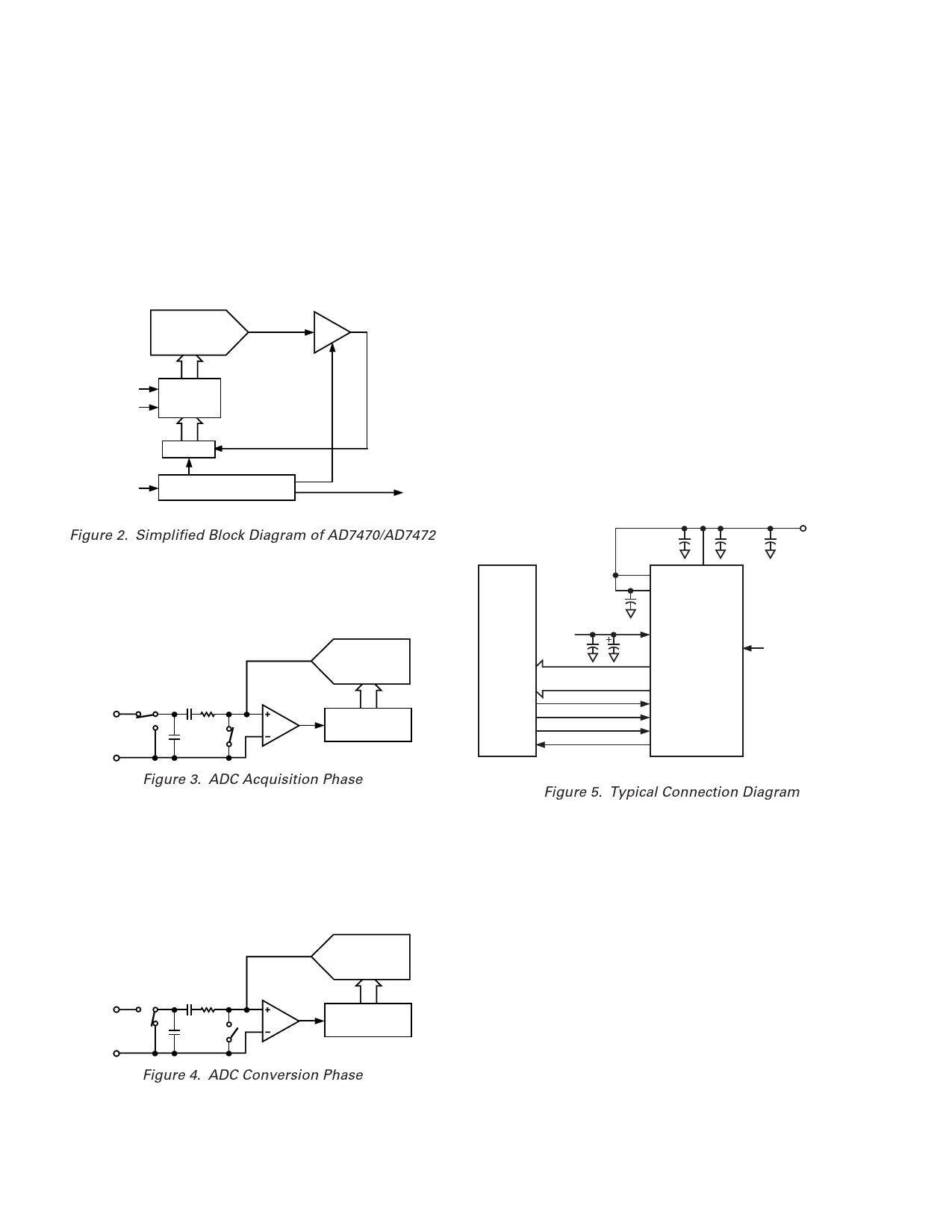
AD7470/AD7472
PARALLEL INTERFACE
The parallel interface of the AD7470 and AD7472 is 10-bits
and 12-bits wide respectively. The output data buffers are acti-
vated when both CS and RD are logic low. At this point the
contents of the data register are placed onto the data bus. Figure
10 shows the timing diagram for the parallel port.
Figure 11 shows the timing diagram for the parallel port when
CS and RD are tied permanently low. In this setup, once the
BUSY line goes from high to low the conversion process is
completed. The data is available on the output bus slightly
before the falling edge of BUSY.
It is important to point out that data bus cannot change state
while the A/D is doing a conversion as this would have a detri-
mental effect on the conversion in progress. The data out lines
will go three-state again when either the RD or CS line goes
high. Thus the CS can be tied low permanently, leaving the RD
line to control conversion result access. Please reference the
VDRIVE section for output voltage levels.
tCONVERT
CONVST*
t2
BUSY
t9
t10
t3
CS
RD
DBx
t4
t8
t5
t6
t7
*CONVST SHOULD GO HIGH WHEN THE CLK IS HIGH OR BEFORE THE FIRST CLK CYCLE.
Figure 10. Parallel Port Timing
tCONVERT
CONVST*
t2
t9
BUSY
DBx
DATA N
DATA N+1
*CONVST SHOULD GO HIGH WHEN THE CLK IS HIGH OR BEFORE THE FIRST CLK CYCLE.
Figure 11. Parallel Port Timing with CS and RD Tied Low
CLK IN
CONVST
BUSY
CS
RD
DBX
tCONVERT
t2
t3
t4
t5
t8
t6
t7
tWAKEUP
Figure 12. Wake-Up Timing Diagram (Burst Clock)
–10–
REV. A
Share Link: 