NIS5112 查看數據表(PDF) - ON Semiconductor
零件编号
产品描述 (功能)
生产厂家
NIS5112 Datasheet PDF : 9 Pages
| |||
NIS5112
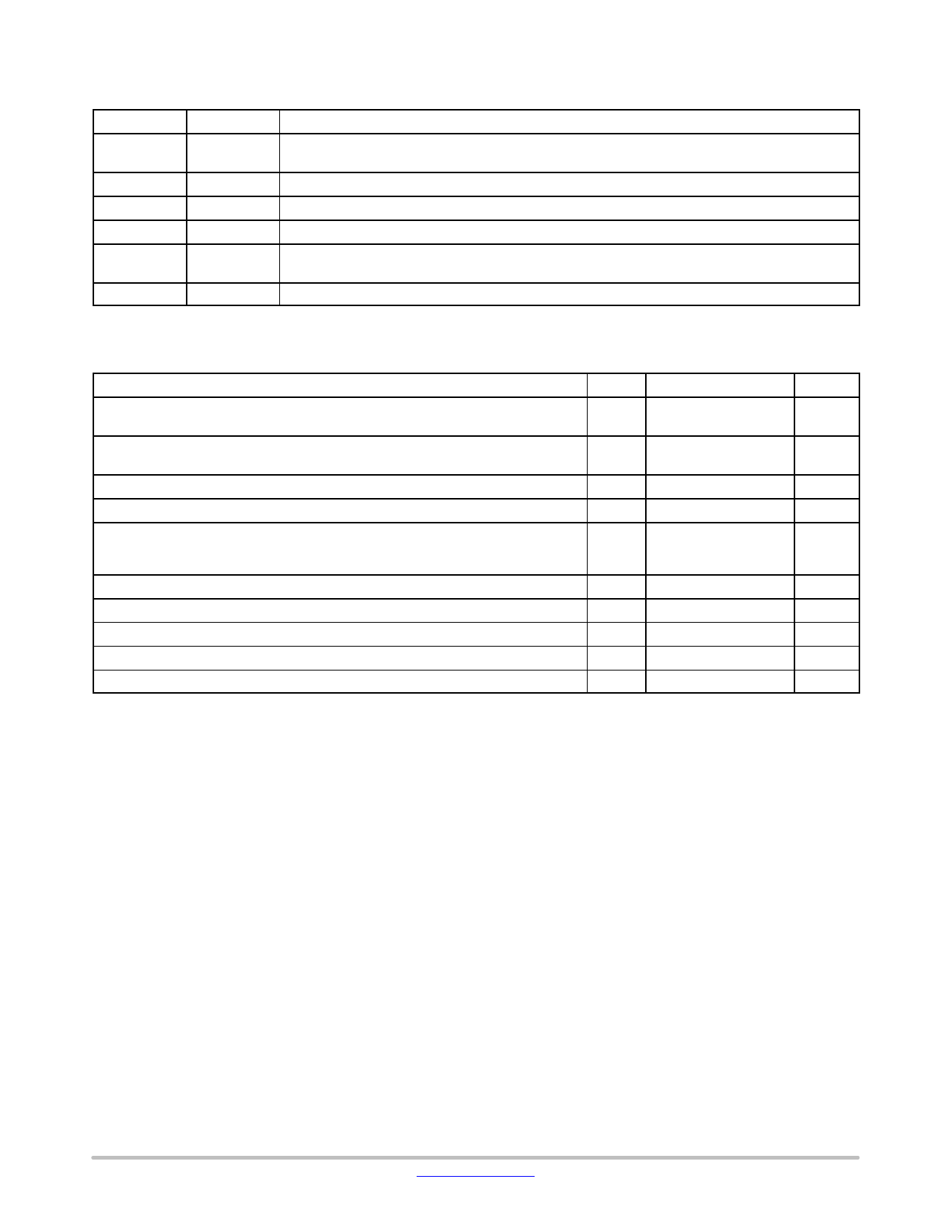
Table 1. FUNCTIONAL PIN DESCRIPTION
Pin
Function
Description
3
Enable/Timer A high level signal on this pin allows the device to begin operation. Connection of a capacitor will delay
turn on for timing purposes. A low input signal inhibits the operation.
1
Ground
Negative input voltage to the device. This is used as the internal reference for the IC.
4
5,6,7
ILimit
Source
A resistor between this pin and the source pin sets the current limit level.
Source of power FET, which is also the switching node for the load.
2
dV/dt
A capacitor from this pin to ground programs the slew rate of the output at turn on. This capacitor is
discharged by an internal discharge circuit when the device is disabled via the enable pin.
8
VCC
Positive input voltage to the device.
Table 2. MAXIMUM RATINGS (Maximum ratings are those, that, if exceeded, may cause damage to the device. Electrical
characteristics are not guaranteed over this range)
Rating
Symbol
Value
Unit
Input Voltage, Operating,
Steady−State (Input+ to Input−)
Vin
−0.3 to 18
V
Transient (Conditions 1 ms)
−0.3 to 25
Drain Voltage, Operating,
Steady−State (Drain to Input−)
VDD
−0.3 to 18
V
Transient (Conditions 1 ms)
−0.3 to 25
Drain Current, Peak (Internally Clamped)
Drain Current, Continuous (TA=25°C), (Note 2)
Thermal Resistance, Junction−to−Air
0.5 in2 Copper
1.0 in2 Copper
IDpk
25
IDavg
5.3
QJA
120
110
A
A
°C/W
°C/W
Thermal Resistance, Junction−to−Lead (Pin 8)
QJL
27
°C/W
Power Dissipation (TA = 25°C) (Note 1)
Pmax
1.0
W
Operating Temperature Range (Note 2)
TJ
−40 to 175
°C
Nonoperating Temperature Range
TJ
−55 to 175
°C
Lead Temperature, Soldering (10 Sec)
TL
260
°C
Stresses exceeding those listed in the Maximum Ratings table may damage the device. If any of these limits are exceeded, device functionality
should not be assumed, damage may occur and reliability may be affected.
1. Mounted on FR−4 board, 1 in sq pad, 1 oz coverage.
2. Actual maximum junction temperature is limited by an internal protection circuit and will not reach the absolute maximum temperature as
specified.
www.onsemi.com
2
Share Link: 