NJM2804 查看數據表(PDF) - Japan Radio Corporation
零件编号
产品描述 (功能)
生产厂家
NJM2804 Datasheet PDF : 5 Pages
| |||
NJM2804
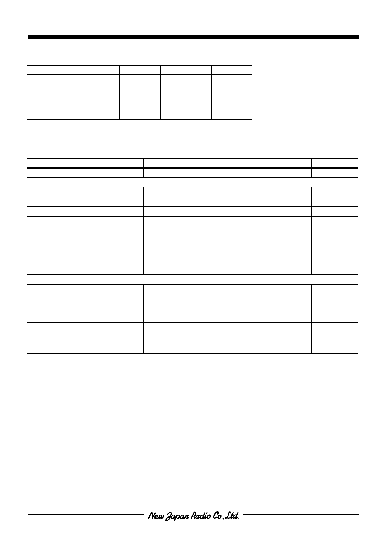
! ABSOLUTE MAXIMUM RATINGS
PARAMETER
SYMBOL
Input Voltage
VIN
Power Dissipation
PD
Operating Temperature
Topr
Storage Temperature
Tstg
RATINGS
+14
350
-40 ∼ +85
-40 ∼ +125
(Ta=25°C)
UNIT
V
mW
°C
°C
! ELECTRICAL CHARACTERISTICS
(VIN=Vo+1V, CIN=0.1µF, Co=1.0µF (Co=2.2µF: Vo≤2.6V) Ta=25°C)
PARAMETER
SYMBOL
TEST CONDITION
MIN. TYP. MAX. UNIT
Quiescent Current
Regulator Block
IQ
VIN=Vo+2V, Io=0mA
−
250 350 µA
Output Voltage
Vo
Io=30mA
-1.0% − +1.0% V
Output Current
Io
Vo-0.3V
300 200
−
mA
Line Regulation
Load Regulation
∆Vo/∆VIN VIN=Vo+1V ∼ Vo+6V, Io=30mA
∆Vo/∆Io Io=0 ∼ 100mA
−
− 0.10 %/V
−
− 0.03 %/mA
Dropout Voltage
∆VI_O Io=60mA
− 0.10 0.18 V
Ripple Rejection
RR ein=200mVrms, f=1kHz, Io=10mA,Vo=3V
−
60
−
dB
Output Voltage
Temperature Coefficient
∆Vo/∆T Ta=0 ∼ 85°C, Io=10mA
− ± 50 − ppm/°C
Output Noise Voltage
Reset Block
VNO
f=10Hz ∼ 100kHz, Io=10mA, Vo=3V
−
45
− µVrms
Voltage Detection
Hysteresis Voltage
Low Level Output Voltage
Output Leak Current
On time Output Current
Reset Output Delay Time
VRT
VRTH
RORL
IORH
IORL
td
VIN=H→L
VIN=H→L→H
VIN=VRT-0.5V, RL=100kΩ
VIN= VRT+0.5V
VIN=VRT-0.5V, RL=0Ω
VIN=(VRT-0.5V)→ (VRT+0.5V), Cd=0.1µF
-1.0% − +1.0% V
VRT×3 VRT×5 VRT×8 mV
−
100 300 mV
−
−
0.1 µA
5
−
−
mA
9
10
11
mS
Operation Voltage Limit
VOPL
VORL=0.4V
−
0.9
−
V
(*note 1): The above specification is a common specification for all output voltages.
Therefore, it may be different from the individual specification for a specific output voltage.
-2-
Ver.2004-01-19
Share Link: 