NJU3426 查看數據表(PDF) - Japan Radio Corporation
零件编号
产品描述 (功能)
生产厂家
NJU3426 Datasheet PDF : 12 Pages
| |||
NJU3426
(4) DISPLAY SHIFT OPERATION
The display shift operation can be performed by changing the “Initial character address” of the “Command register 2”.
And, the number of digits for the display shift in the loop is determined by the “Shifting display digits” of the
“Command register 1”. In other words, shifting display area ranges from the “Initial character address” specified by the
“Command register 2” to the last address designated by the “Command register 1”.
The default value of the “Initial character address” is C1 (0,0,0,1), as shown in the table of “Display data RAM”. In
addition, supposing that the value of the “Shifting display digits” is “N”, the “Initial character address” must be set in the
range between C0 and CN in order not to exceed the digit “N”. Because the display shift operation doesn’t apply to the
addresses beyond the range of the digit “N”, the display images, initially set, appear on these addresses. Just for
reference, one character of display image is composed of 16 segments.
HOW TO SET LEFT DISPLAY SHIFT
The left display shift is carried out by incrementing the “Initial character address” gradually like C2, C3, C4, ---
CN. To the contrary, decrementing the address performs right display shift. The following description
provides the example on how to set the left display shift, using alphanumeric display images such as “0”, “1”,
“2”, ---, “9”, “A”, “B”, ---, and “E”.
STEP1) Setting display images in the display data RAM
• Display RAM data
Character address
Display image
C0 C1 C2 C3 C4 C5 C6 C7 C8 C9 C10 C11 C12 C13 C14
0 1 2 3 4 5 6 7 8 9ABCDE
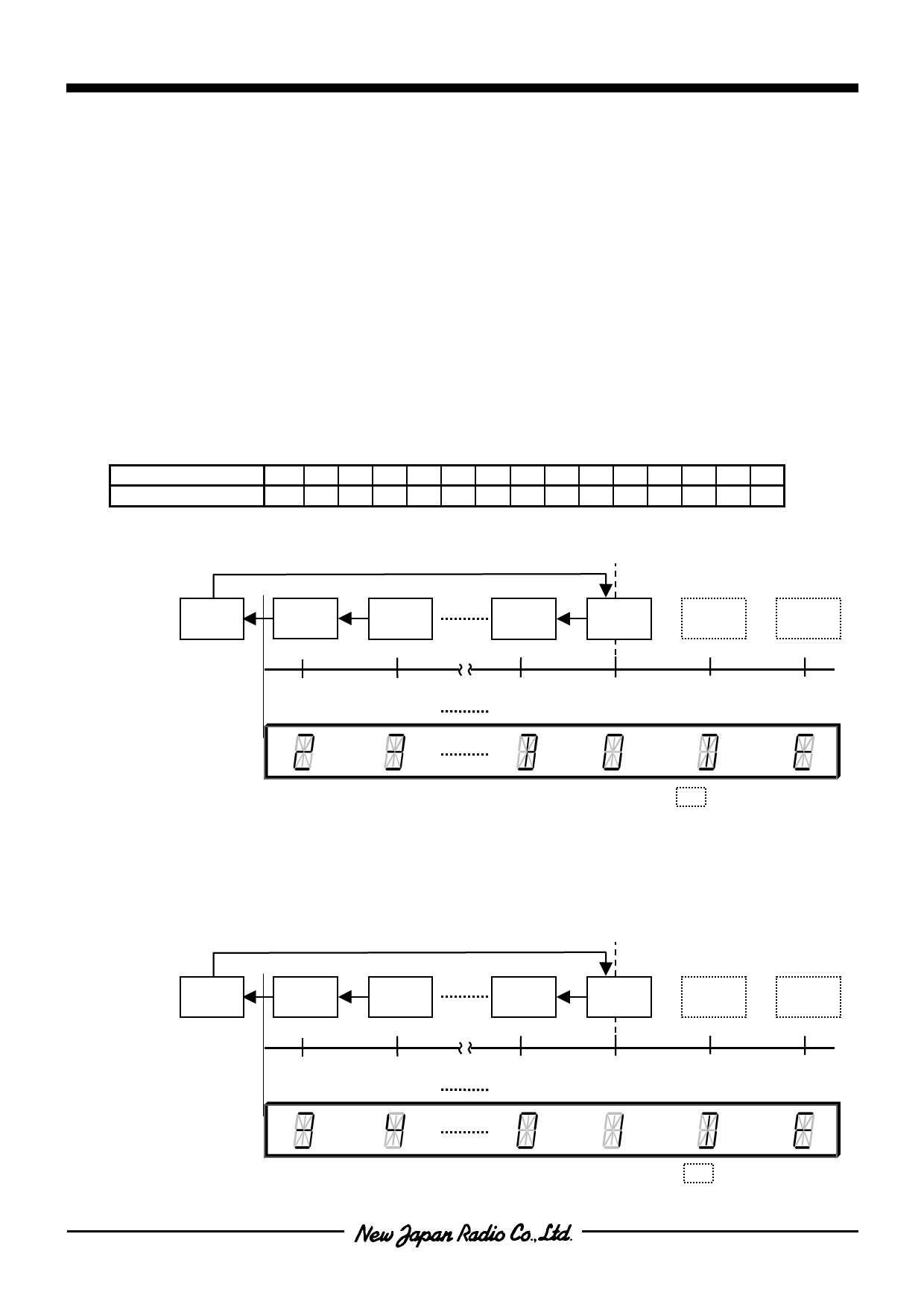
SETP2) Setting the “Initial character address” to C2 and the “Shifting display digits N” to 12 (T11).
Shifting display digits
Character
C1
C2
C3
address
Timing output
terminals
Character
T0
T1
1
2
Display image
C12
C0
C13
C14
T10
T11
T12
T13
11
12
13
14
is not shifted.
In this setting, the display images of "2", "3”,- - - appear on the T0, T1, T2, - - - T10 pins respectively, and the
image “0” is on the T11 pin, which is assigned to the 12th character address. The display images “D” and “E”
don’t shift but remain on the T12 and T13 pins, assigned to the 13th and 14th characters respectively, because their
character addresses are outside of the digit “N”.
STEP3) Changing the “Initial character address” to C3, and leaving the “Shifting display digits N” as 12 (T11).
Shifting display digits
Character
C2
C3
C4
address
Timing output
terminals
Character
T0
T1
1
2
Display image
C0
C1
C13
C14
T10
T11
T12
T13
11
12
13
14
is not shifted.
-5-
Share Link: 