NJU3426 查看數據表(PDF) - Japan Radio Corporation
零件编号
产品描述 (功能)
生产厂家
NJU3426 Datasheet PDF : 12 Pages
| |||
NJU3426
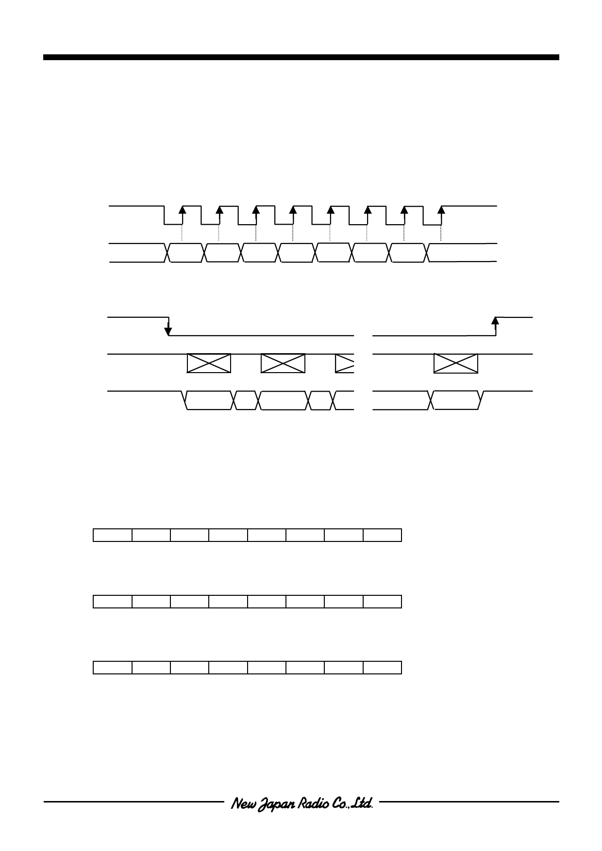
(5) SERIAL DATA TRANSMISSION
Communication between the NJU3426 and MPU uses the serial data transmission with synchronous clock, and 8 bits
serial data constitutes 1 word. Each bit on the SI pin is fetched at the rising edge of the serial clock (SCK), and the
entire 8 bits are loaded as 1 word at the rising edge of the chip select (CSb).
During one communication, multiple words can be transferred continuously. The 1st word must be either “Display data
RAM address”, “Command register 1” or “Command register 2”. When the 1st word is RAM address data, the 2nd and
ascending words must be display data. When it’s the “Command register 1 or 2”, the 2nd and ascending words are
ignored.
SCK
SI
D0 D1
D2 D3 D4 D5
D6
D7
SERIAL DATA TIMING
CSb
SCK
SI
WORD 1
WORD 2
WORD n
SERIAL DATA TRANSMISSION FORMAT
• Serial input data
DATA FORMAT FOR THE 1ST WORD
DISPLAY DATA RAM ADRESS
B7
B6
B5
B4
B3
B2
B1
B0
0
0
*
AD4 AD3 AD2 AD1 AD0
*:don’t care
COMMAND DATA 1
B7
B6
B5
B4
B3
B2
B1
B0
1
DT2 DT1 DT0 DSP DE2 DE1 DE0
*:don’t care
COMMAND DATA 2
B7
B6
B5
0
1
*
B4
B3
B2
B1
B0
*
DS3 DS2 DS1 DS0
*:don’t care
SERIAL DATA FOR THE 2ND AND ASCENDING WORDS
When the 1st word is the “Display data RAM address”, the 2nd and ascending words must be display data.
When the 1st word is the “Command register 1 or 2”, the 2nd and ascending words are ignored.
-7-
Share Link: 