NJU8721 查看數據表(PDF) - Japan Radio Corporation
零件编号
产品描述 (功能)
生产厂家
NJU8721 Datasheet PDF : 13 Pages
| |||
NJU8721
! TERMINAL DESCRIPTION
No.
SYMBOL
I/O FUNCTION
1
STBY
I
Standby Control Terminal
Low : Standby ON
High : Standby OFF
2
TEST
I
Manufacturer Testing Terminal
Normally connect to GND.
3
VSSR
− Rch Power GND, VSSR=0V
4
OUTR
O Rch Output Terminal
5
VDDR
− Rch Power Supply, VDDR=VDD to 5.0V
6
VDDL
− Lch Power Supply, VDDL=VDD to 5.0V
7
OUTL
O Lch Output terminal
8
VSSL
− Lch Power GND, VSSL=0V
9
MODE
I
Control Mode selection Terminal
Low : Parallel Control Mode
High : Serial Control Mode
10
RST
I
Reset Terminal
Low : Reset ON
High : Reset OFF
11
VSS
− Logic Power GND, VSS=0V
12
MCK
I
Master Clock Input Terminal
256fS clock inputs this terminal.
13
BCK
I
Serial Audio Data Bit Clock Input Terminal
This clock must synchronize with MCK input signal.
14
LRCK
I
L/R Channel Clock Input Terminal
This clock must synchronize with MCK input signal.
15
DIN
I Serial Audio Data Input Terminal
16
MUTE
I
Mute Control Terminal
Low : Mute ON
High : Mute OFF
MODE=”Low” : Serial Audio Interface Format Selection Terminal 2
17
F2/SCK
I
MODE=”High” : Control Register Data Shift Clock Input Terminal
The data is fetched into the control register by rise edge of SCK
signal.
18
F1/REQ
I
MODE=”Low”
MODE=”High”
: Serial Audio Interface Format Selection Terminal 1
: Control Register Data Request Input Terminal
19
F0/DATA
I
MODE=”Low”
MODE=”High”
: Serial Audio Interface Format Selection Terminal 0
: Control Register Data Input Terminal
20
VDD
− Logic Power Supply, VDD=3.3V
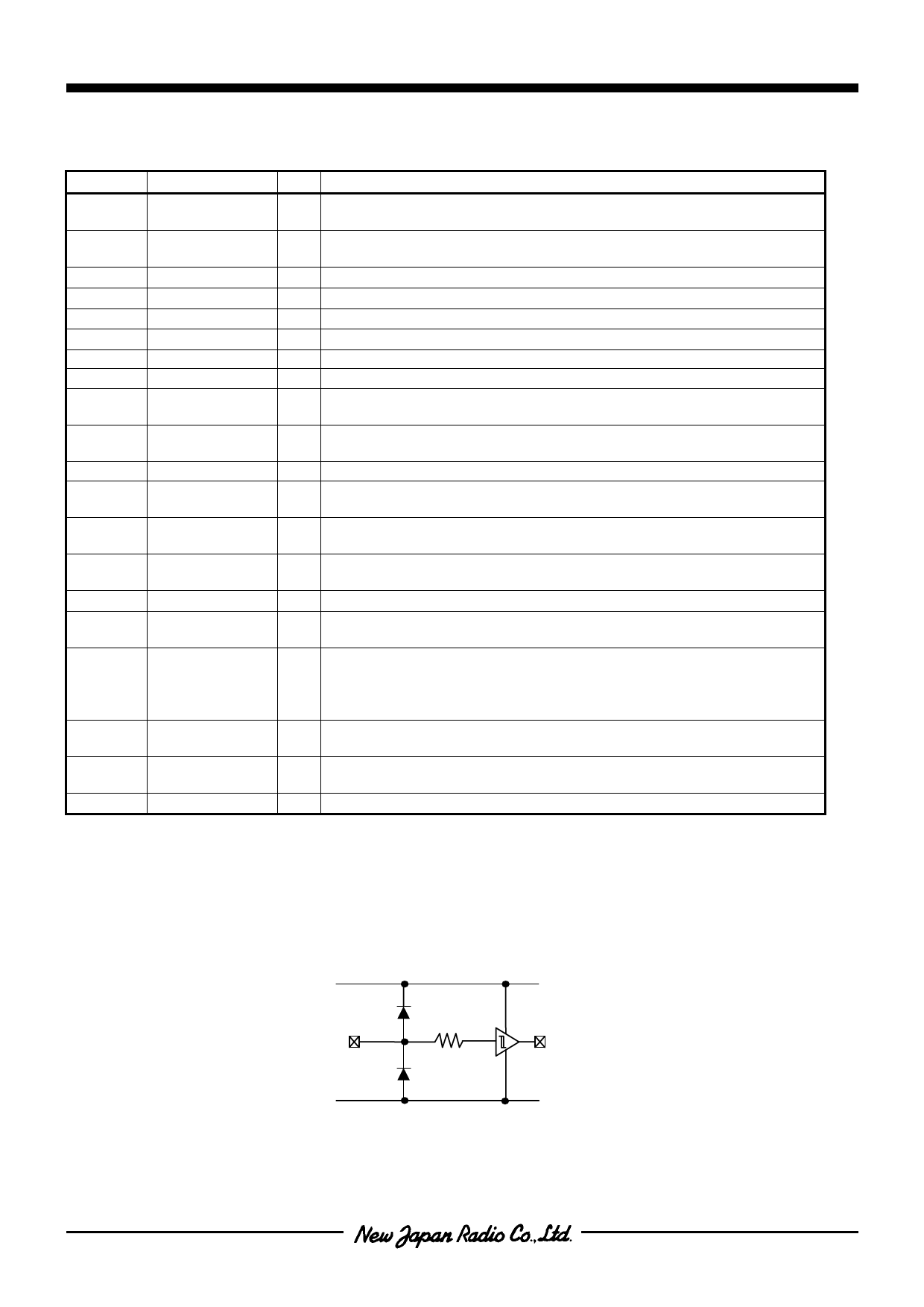
! INPUT TERMINAL STRUCTURE
VDD
Input Terminal
VSS
Inside Circuit
-2-
Share Link: 