NLSX3012 查看數據表(PDF) - ON Semiconductor
零件编号
产品描述 (功能)
生产厂家
NLSX3012 Datasheet PDF : 12 Pages
| |||
NLSX3012
ENABLE / DISABLE TIME MEASUREMENTS
−405C to +855C
Symbol
Parameter
Test Conditions
(Note 13)
VCC (V)
(Note 14)
VL (V)
(Note 15)
Typ
Min (Note 16) Max Unit
tEN−VCC Turn−On Enable Time (Output =
I/O_VCC, tpZH)
CIOVCC = 15 pF 1.3 to 4.5 0.9 to (VCC – 0.4)
150
200 ns
tEN−VL
Turn−On Enable Time (Output =
I/O_VCC, tpZL)
Turn−On Enable Time (Output =
I/O_VL, tpZH)
Turn−On Enable Time (Output =
I/O_VL, tpZL)
CIOVL = 15 pF
CIOVCC = 15 pF
CIOVL = 15 pF
1.3 to 4.5 0.9 to (VCC – 0.4)
1.3 to 4.5 0.9 to (VCC – 0.4)
1.3 to 4.5 0.9 to (VCC – 0.4)
130
180 ns
95
225 ns
75
100 ns
tDIS−VCC Turn−Off Disable Time (Output =
I/O_VCC, tpHZ)
CIOVCC = 15 pF 1.3 to 4.5 0.9 to (VCC – 0.4)
175
250 ns
Propagation Delay (Output =
I/O_VCC, tPLZ)
CIOVL = 15 pF
1.3 to 4.5 0.9 to (VCC – 0.4)
140
160 ns
tDIS−VL Turn−Off Disable Time (Output =
I/O_VL, tpHZ)
CIOVCC = 15 pF 1.3 to 4.5 0.9 to (VCC – 0.4)
180
275 ns
Propagation Delay (Output = I/O_VL,
tPLZ)
CIOVL = 15 pF
1.3 to 4.5 0.9 to (VCC – 0.4)
160
220 ns
13. Normal test conditions are VEN = 0 V, CIOVCC = 15 pF and CIOVL = 15 pF, unless otherwise specified.
14. VCC is the supply voltage associated with the high voltage port, and VCC ranges from +1.3 V to 4.5 V under normal operating conditions.
15. VL is the supply voltage associated with the low voltage port. VL must be less than or equal to (VCC – 0.4) V during normal operation. However,
during startup and shutdown conditions, VL can be greater than (VCC – 0.4) V.
16. Typical values are for VCC = +2.8 V, VL = +1.8 V and TA = +25 °C. All units are production tested at TA = +25 °C. Limits over the operating
temperature range are guaranteed by design.
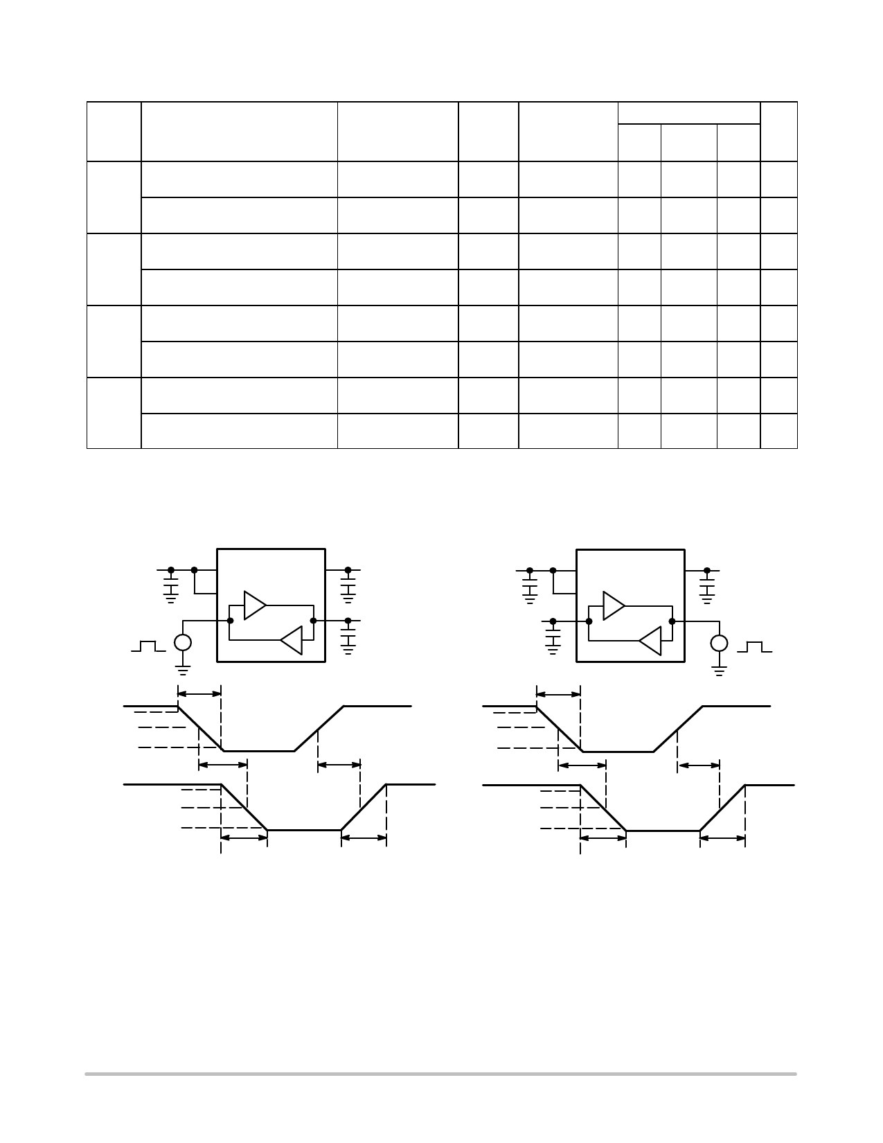
VL
Source
NLSX3012
EN
I/O VL
VCC
I/O VCC
CIOVCC
I/O VL
90%
50%
10%
I/O VCCtPD_VL−VCC
90%
50%
10%
tRISE/FALL v
3 ns
tF−VCC
tPD_VL−VCC
tR−VCC
Figure 3. Driving I/O VL Test Circuit and Timing
VL
I/O VL
CIOVL
NLSX3012
EN
I/O VCC
90%
50%
10%
I/O VLtPD_VCC−VL
90%
50%
10%
tRISE/FALL v 3 ns
tF−VL
VCC
I/O VCC
Source
tPD_VCC−VL
tR−VL
Figure 4. Driving I/O VCC Test Circuit and Timing
http://onsemi.com
7
Share Link: 