SPT7862 查看數據表(PDF) - Signal Processing Technologies
零件编号
产品描述 (功能)
生产厂家
SPT7862 Datasheet PDF : 10 Pages
| |||

ANALOG INPUT
VINA and VINB are the analog inputs and VINRA and VINRB are
the respective input returns. Each input return is typically
tied to its respective low side reference ladder sense line.
(See Figure 2.) The input voltage range is from VRLS to VRHS
(typically 4.0 V) and will scale proportionally with respect to
the voltage reference. (See the Voltage Reference section.)
The drive requirements for the analog inputs are very mini-
mal, when compared to most other converters, due to the
SPT7862’s extremely low input capacitance of only 5 pF
and a high input resistance in excess of 29 kΩ.
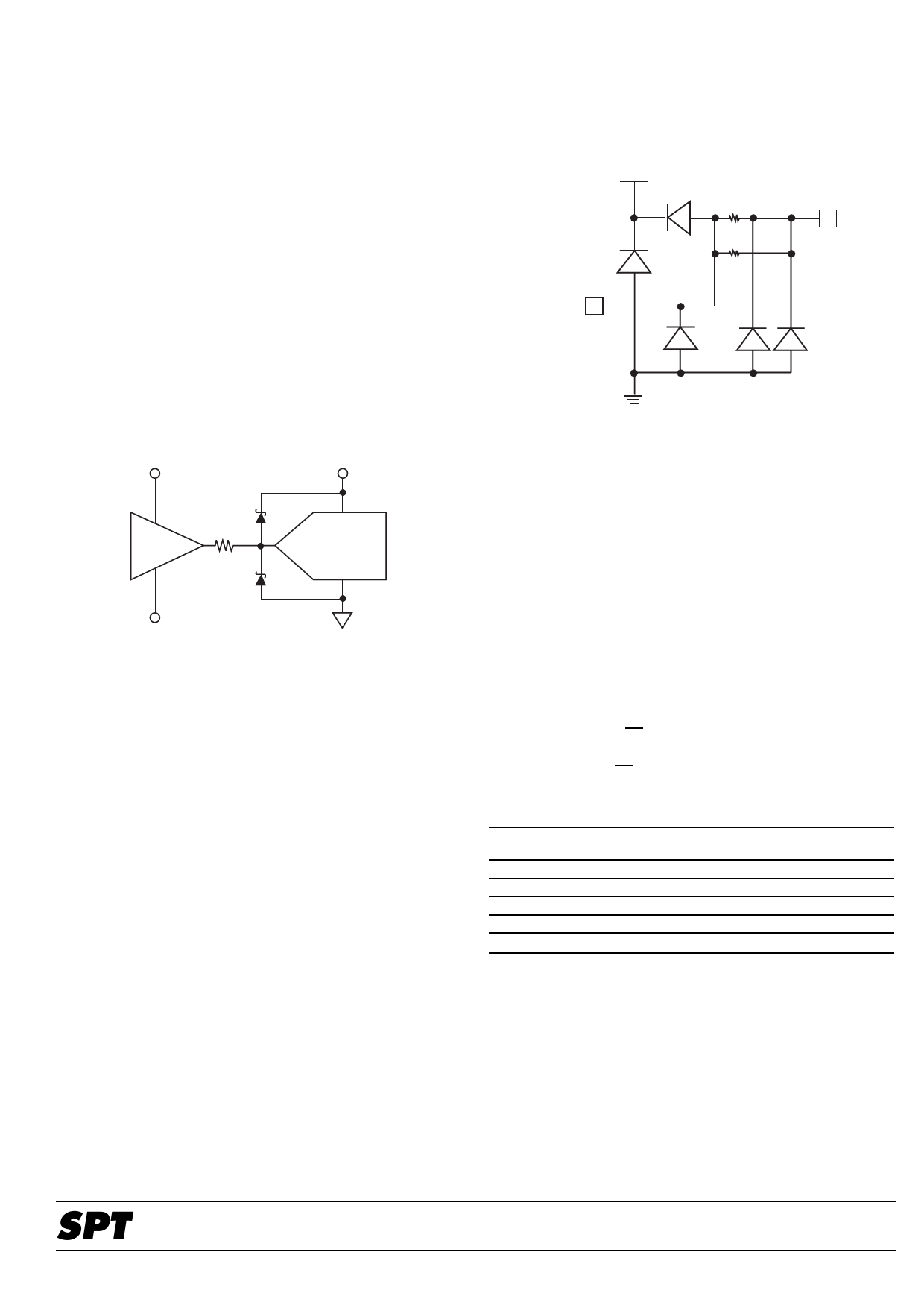
Each analog input should be protected through a series
resistor and diode clamping circuit as shown in figure 5.
Figure 5 – Recommended Input Protection Circuit
+V
AVDD
Buffer
D1
47 Ω
D2
ADC
–V
D1 = D2 = Hewlett Packard HP5712 or equivalent
CALIBRATION
The SPT7862 uses a user-transparent, auto-calibration
scheme to ensure 10-bit accuracy over time and tempera-
ture. Gain and offset errors are continually adjusted to 10-bit
accuracy during device operation.
Upon power up, the SPT7862 begins its calibration algo-
rithm. In order to achieve the calibration accuracy required,
the offset and gain adjustment step size is a fraction of a 10-
bit LSB. Since the calibration algorithm is an oversampling
process, a minimum of 10,000 clock cycles are required.
This results in a minimum calibration time upon power up of
250 µsec (for a 40 MHz clock). Once calibrated, the
SPT7862 remains calibrated over time and temperature.
Since the calibration cycles are initiated on the rising edge
of the clock, the clock must be continuously applied for the
SPT7862 to remain in calibration.
INPUT PROTECTION
All I/O pads are protected with an on-chip protection circuit
shown in figure 6. This circuit provides ESD robustness and
prevents latch-up under severe discharge conditions with-
out degrading analog transition times.
Figure 6 – On-Chip Protection Circuit
VDD
120 Ω
Analog
120 Ω
Pad
CLOCK INPUT
Each ADC is driven independently from a single-ended
TTL-input clock. Because the pipelined architecture oper-
ates on the rising edge of the clock input, each ADC can
operate over a wide range of input clock duty cycles without
degrading the dynamic performance.
DIGITAL OUTPUTS
The digital outputs (DA9–0 and DB9–0) are driven by sepa-
rate supplies (OVDDA and OVDDB) ranging from +3 V to
+5 V. This feature makes it possible to drive the SPT7862’s
TTL/CMOS-compatible outputs with the user’s logic system
supply. Each digital output supply may be driven indepen-
dently. The format of the output data (D0–D9) is straight
binary. (See Table III.) The outputs are latched on the rising
edge of CLK. The EN pin controls tri-stating of both data
output ports. These outputs can be switched into a tri-state
mode by bringing EN high.
Table III – Output Data Information
ANALOG INPUT
+F.S. + 1/2 LSB
+F.S. –1/2 LSB
+1/2 F.S.
+1/2 LSB
OVERRANGE
D10
1
0
0
0
OUTPUT CODE
D9–D0
11 1111 1111
11 1111 111Ø
ØØ ØØØØ ØØØØ
00 0000 000Ø
0.0 V
0
00 0000 0000
(Ø indicates the flickering bit between logic 0 and 1)
EVALUATION BOARD
The EB7862 evaluation board is available to aid designers
in demonstrating the full performance of the SPT7862.
This board includes a reference circuit, clock driver circuit,
output data latches and an on-board reconstruction of the
digital data. An application note describing the operation of
this board as well as information on the testing of the
SPT7862 is also available. Contact the factory for price and
availability.
SPT
8
SPT7862
2/23/00