NMC27C32B 查看數據表(PDF) - Fairchild Semiconductor
零件编号
产品描述 (功能)
生产厂家
NMC27C32B Datasheet PDF : 10 Pages
| |||
Functional Description
DEVICE OPERATION
The six modes of operation of the NMC27C32B are listed in
Table I A single 5V power supply is required in the read
mode All inputs are TTL levels except for OE VPP during
programming In the program mode the OE VPP input is
pulsed from a TTL low level to 12 75V
Read Mode
The NMC27C32B has two control functions both of which
must be logically active in order to obtain data at the out-
puts Chip Enable (CE) is the power control and should be
used for device selection Output Enable (OE) is the output
control and should be used to gate data to the output pins
independent of device selection Assuming that addresses
are stable address access time (tACC) is equal to the delay
from CE to output (tCE) Data is available at the outputs tOE
after the falling edge of OE assuming that CE has been low
and addresses have been stable for at least tACC – tOE
The sense amps are clocked for fast access time VCC
should therefore be maintained at operating voltage during
read and verify If VCC temporarily drops below the spec
voltage (but not to ground) an address transition must be
performed after the drop to ensure proper output data
Standby Mode
The NMC27C32B has a standby mode which reduces the
active power dissipation by 99% from 55 mW to 0 55 mW
The NMC27C32B is placed in the standby mode by applying
a CMOS high signal to the CE input When in standby mode
the outputs are in a high impedance state independent of
the OE input
Output OR-Tying
Because EPROMs are usually used in larger memory ar-
rays National has provided a 2-line control function that
accommodates this use of multiple memory connection
The 2-line control function allows for
a The lowest possible memory power dissipation and
b complete assurance that output bus contention will not
occur
To most efficiently use these two control lines it is recom-
mended that CE (pin 18) be decoded and used as the pri-
mary device selecting function while OE (pin 20) be made a
common connection to all devices in the array and connect-
ed to the READ line from the system control bus This as-
sures that all deselected memory devices are in their low
power standby modes and that the output pins are active
only when data is desired from a particular memory device
Programming
CAUTION Exceeding 14V on pin 20 OE VPP will damage
the NMC27C32B
Initially and after each erasure all bits of the NMC27C32B
are in the ‘‘1’’ state Data is introduced by selectively pro-
gramming ‘‘0s’’ into the desired bit locations Although only
‘‘0s’’ will be programmed both ‘‘1s’’ and ‘‘0s’’ can be pre-
sented in the data word The only way to change a ‘‘0’’ to a
‘‘1’’ is by ultraviolet light erasure
The NMC27C32B is in the programming mode when
OE VPP is at 12 75V It is required that at least a 0 1 mF
capacitor be placed across VCC and ground to suppress
spurious voltage transients which may damage the device
The data to be programmed is applied 8 bits in parallel to
the data output pins The levels required for the address
and data inputs are TTL
When the address and data are stable an active low TTL
program pulse is applied to the CE input A program pulse
must be applied at each address location to be pro-
grammed The NMC27C32B is programmed with the Fast
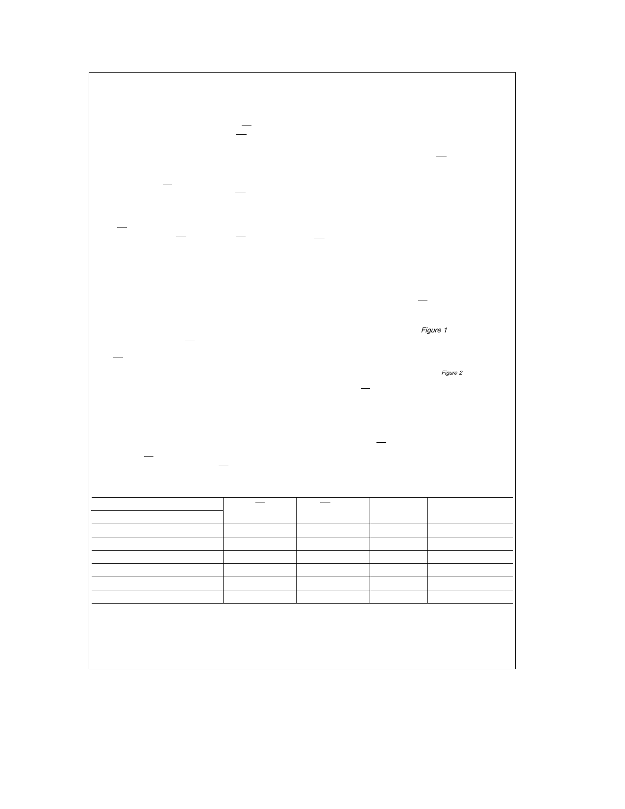
Programming Algorithm shown in Figure 1 Each Address is
programmed with a series of 100 ms pulses until it verifies
good up to a maximum of 25 pulses Most memory cells will
Program with a single 100 ms pulse
Note Some programmer manufactures due to equipment limitation may of-
fer interactive program Algorithm (Shown in Figure 2 )
The NMC27C32B must not be programmed with a DC signal
applied to the CE input
Programming multiple NMC27C32Bs in parallel with the
same data can be easily accomplished due to the simplicity
of the programming requirements Like inputs of the paral-
leled NMC27C32B may be connected together when they
are programmed with the same data A low level TTL pulse
applied to the CE input programs the paralleled
NMC27C32B
Mode
Read
Standby
Program
Program Verify
Program Inhibit
Output Disable
Pins
TABLE I Mode Selection
CE
(18)
VIL
VIH
VIL
VIL
VIH
Don’t Care
OE VPP
(20)
VIL
Don’t Care
12 75V
VIL
12 75V
VIH
VCC
(24)
5V
5V
6 25V
6 25V
6 25V
5V
Outputs
(9 – 11 13 – 17)
DOUT
Hi-Z
DIN
DOUT
Hi-Z
Hi-Z
7
http www national com
Share Link: 