NMC27C32B 查看數據表(PDF) - Fairchild Semiconductor
零件编号
产品描述 (功能)
生产厂家
NMC27C32B Datasheet PDF : 10 Pages
| |||
Functional Description (Continued)
Program Inhibit
Programming multiple NMC27C32B in parallel with different
data is also easily accomplished Except for CE all like in-
puts (including OE) of the parallel NMC27C32B may be
common A TTL low level program pulse applied to an
NMC27C32B’s CE input with OE VPP at 12 75V will pro-
gram that NMC27C32B A TTL high level CE input inhibits
the other NMC27C32B from being programmed
Program Verify
A verify should be performed on the programmed bit to de-
termine whether they were correctly programmed The veri-
fy is accomplished with OE VPP and CE at VIL Data should
be verified tDV after the falling edge of CE
MANUFACTURER’S IDENTIFICATION CODE
The NMC27C32B has a manufacturer’s identification code
to aid in programming The code shown in Table II is two
bytes wide and is stored in a ROM configuration on the chip
It identifies the manufacturer and the device type The code
for the NMC27C32B is ‘‘8F01’’ where ‘‘8F’’ designates that
it is made by National Semiconductor and ‘‘01’’ designates
a 32k part
The code is accessed by applying 12 0V g0 5V to address
pin A9 Addresses A1–A8 A10–A11 CE and OE are held
at VIL Address A0 is held at VIL for the manufacturer’s
code and at VIH for the device code The code is read out
on the 8 data pins Proper code access is only guaranteed
at 25 C g5 C
The primary purpose of the manufacturer’s identification
code is automatic programming control When the device is
inserted in an EPROM programmer socket the programmer
reads the code and then automatically calls up the specific
programming algorithm for the part This automatic pro-
gramming control is only possible with programmers which
have the capability of reading the code
ERASURE CHARACTERISTICS
The erasure characteristics of the NMC27C32B are such
that erasure begins to occur when exposed to light with
wavelengths shorter than approximately 4000 Angstroms
( ) It should be noted that sunlight and certain types of
fluorescent lamps have wavelengths in the 3000 – 4000
range After programming opaque labels should be placed
over the NMC27C32B’s window to prevent unintentional
erasure Covering the window will also prevent temporary
functional failure due to the generation of photo currents
The recommended erasure procedure for the NMC27C32B
is exposure to short wave ultraviolet light which has a wave-
length of 2537 The integrated dose (i e UV intensity c
exposure time) for erasure should be a minimum of
15 W-sec cm2
The NMC27C32B should be placed within 1 inch of the
lamp tubes during erasure Some lamps have a filter on their
tubes which should be removed before erasure Table III
shows the minimum NMC27C32B erasure time for various
light intensities
An erasure system should be calibrated periodically The
distance from lamp to unit should be maintained at one inch
The erasure time increases as the square of the distance (If
distance is doubled the erasure time increases by a factor of
4 ) Lamps lose intensity as they age When a lamp is
changed the distance has changed or the lamp has aged
the system should be checked to make certain full erasure
is occurring Incomplete erasure will cause symptoms that
can be misleading Programmers components and even
system designs have been erroneously suspected when in-
complete erasure was the problem
SYSTEM CONSIDERATION
The power switching characteristics of EPROMs require
careful decoupling of the devices The supply current ICC
has three segments that are of interest to the system de-
signer the standby current level the active current level
and the transient current peaks that are produced by volt-
age transitions on input pins The magnitude of these tran-
sient current peaks is dependent on the output capacitance
loading of the device The associated VCC transient voltage
peaks can be suppressed by properly selected decoupling
capacitors It is recommended that at least a 0 1 mF ceramic
capacitor be used on every device between VCC and GND
This should be a high frequency capacitor of low inherent
inductance In addition at least a 4 7 mF bulk electrolytic
capacitor should be used between VCC and GND for each
eight devices The bulk capacitor should be located near
where the power supply is connected to the array The pur-
pose of the bulk capacitor is to overcome the voltage drop
caused by the inductive effects of the PC board traces
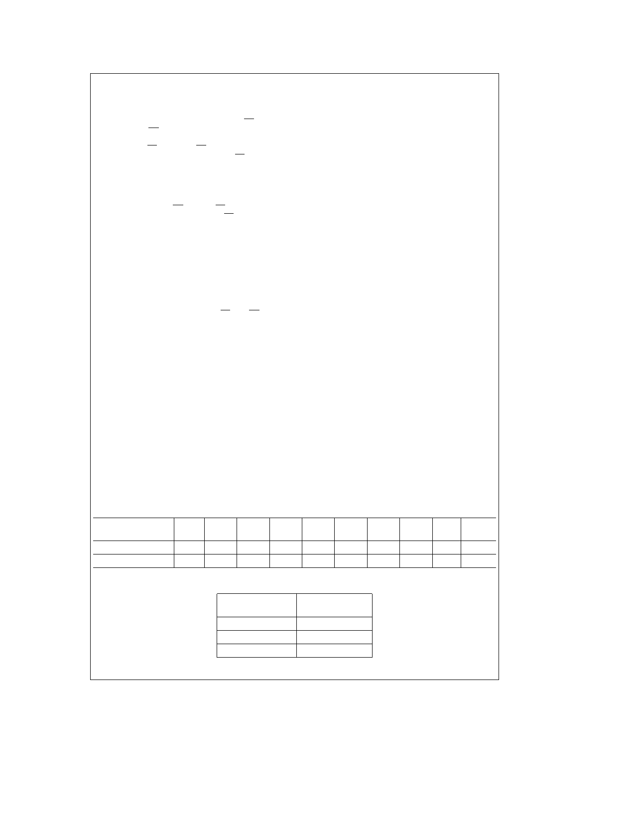
TABLE II Manufacturer’s Identification Code
Pins
A0
O7
O6
O5
O4
O3
O2
O1
O0
Hex
(8)
(17)
(16)
(15)
(14)
(13)
(11)
(10)
(9)
Data
Manufacturer Code
VIL
1
0
0
0
1
1
1
1
8F
Device Code
VIH
0
0
0
0
0
0
0
1
01
TABLE III Minimum NMC27C32B Erasure Time
Light Intensity
(mW cm2)
Erasure Time
(Minutes)
15 000
20
10 000
25
5 000
50
http www national com
8
Share Link: 