NP1800SAMCT3G 查看數據表(PDF) - ON Semiconductor
零件编号
产品描述 (功能)
生产厂家
NP1800SAMCT3G Datasheet PDF : 7 Pages
| |||
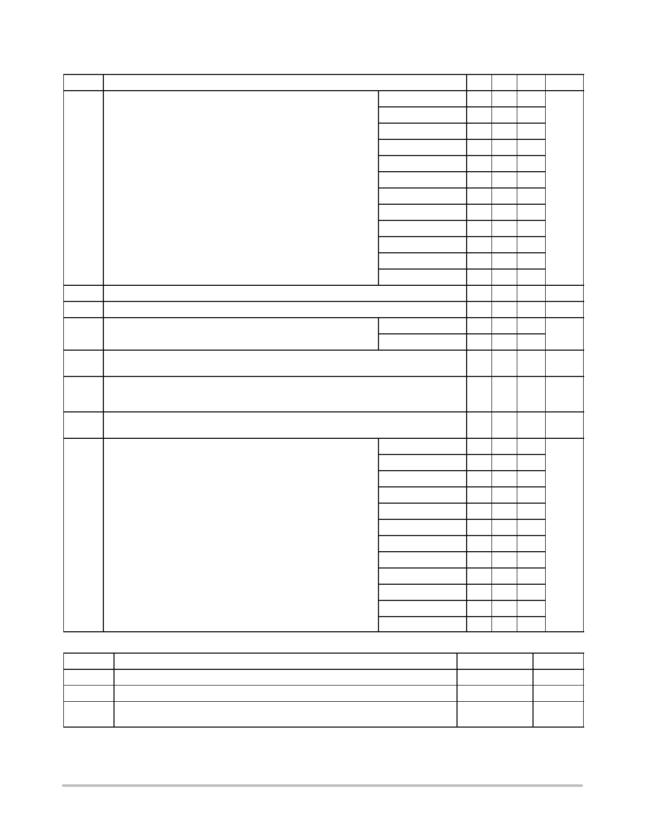
NP−SAMC Series
ELECTRICAL CHARACTERISTICS TABLE (TA = 25°C unless otherwise noted)
Symbol
Rating
Min Typ Max Unit
V(BO)
Breakover voltage: The maximum voltage across the device in or at the
breakdown region.
VDC = 1000 V, dv/dt = 100 V/ms
NP0640SAMCT3G
NP0720SAMCT3G
NP0900SAMCT3G
$77 V
$88
$98
NP1100SAMCT3G
$130
NP1300SAMCT3G
$160
NP1500SAMCT3G
$180
NP1800SAMCT3G
$220
NP2100SAMCT3G
$240
NP2300SAMCT3G
$260
NP2600SAMCT3G
$300
NP3100SAMCT3G
$350
NP3500SAMCT3G
$400
I(BO)
IH
IDRM
VT
dv/dt
di/dt
Breakover Current: The instantaneous current flowing at the breakover voltage.
Holding Current: The minimum current required to maintain the device in the on−state.
150
Off−state Current: The dc value of current that results from the applica- VD = 50 V
tion of the off−state voltage
VD = VDRM
On−state Voltage: The voltage across the device in the on−state condition.
IT = 2.2 A (pk), PW = 300 ms, DC = 2%
Critical rate of rise of off−state voltage: The maximum rate of rise of voltage (below VDRM) that ±5
will not cause switching from the off−state to the on−state.
Linear Ramp between 0.1 VDRM and 0.9 VDRM
Critical rate of rise of on−state current: rated value of the rate of rise of current which the device
can withstand without damage.
800 mA
mA
2
mA
5
4
V
kV/ms
±500 A/ms
CO Off−state Capacitance
f = 1.0 MHz, Vd = 1.0 VRMS, VD = −2 Vdc
NP0640SAMCT3G
NP0720SAMCT3G
18
pF
18
NP0900SAMCT3G
18
NP1100SAMCT3G
18
NP1300SAMCT3G
18
NP1500SAMCT3G
18
NP1800SAMCT3G
18
NP2100SAMCT3G
18
NP2300SAMCT3G
18
NP2600SAMCT3G
18
NP3100SAMCT3G
18
NP3500SAMCT3G
18
THERMAL CHARACTERISTICS
Symbol
Rating
TSTG
TJ
R0JA
Storage Temperature Range
Junction Temperature
Thermal Resistance: Junction−to−Ambient Per EIA/JESD51−3, PCB = FR4 3”x4.5”x0.06”
Fan out in a 3x3 inch pattern, 2 oz copper track.
Value
−65 to +150
−40 to +150
90
Unit
°C
°C
°C/W
http://onsemi.com
3
Share Link: 