AD8184 查看數據表(PDF) - Analog Devices
零件编号
产品描述 (功能)
生产厂家
AD8184 Datasheet PDF : 12 Pages
| |||
AD8184
Chip capacitors should be used for supply bypassing. One end
of the capacitor should be connected to the ground plane and
the other within 1/4 inch of each power pin. An additional large
(4.7 µF–10 µF) tantalum capacitor should be connected in par-
allel with each of the smaller capacitors for low impedance sup-
ply bypassing over a broad range of frequencies.
Signal traces should be as short as possible. Stripline or
microstrip techniques should be used for long (longer than
about 1 inch) signal traces. These should be designed with a
characteristic impedance of 50 Ω or 75 Ω and be properly ter-
minated at each end using surface mount components.
Careful layout is imperative to minimize crosstalk. Guards
(ground or supply traces) must be run between all signal traces
to limit direct capacitive coupling. Input and output signal lines
should fan out away from the mux as much as possible. If mul-
tiple signal layers are available, a buried stripline structure hav-
ing ground plane above, below and between signal traces will
have the best crosstalk performance.
Return currents flowing through termination resistors can also
increase crosstalk if these currents flow in sections of the finite-
impedance ground circuit shared between more than one input
or output. Minimizing the inductance and resistance of the ground
plane can reduce this effect, but further care should be taken in po-
sitioning the terminations. Terminating cables directly at the con-
nectors will minimize the return current flowing on the board, but
the signal trace between the connector and the mux will look like
an open stub and will degrade the frequency response. Moving the
termination resistors close to the input pins will improve the fre-
quency response, but the terminations from neighboring inputs
should not have a common ground return.
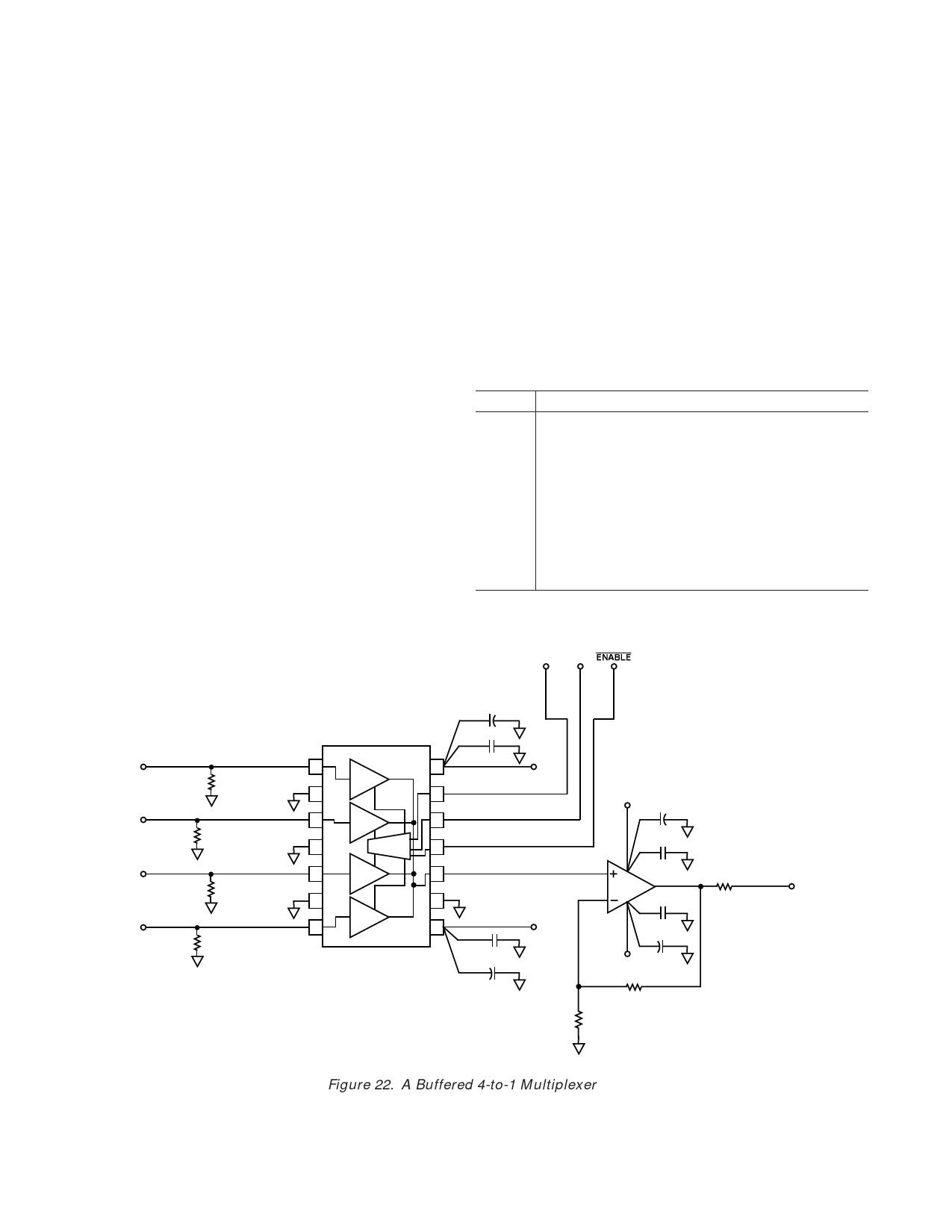
APPLICATIONS
A Buffered 4-to-1 Multiplexer
In applications where the output of a multiplexer must drive a
back-terminated 75 Ω line (RL = 75 Ω + 75 Ω), it is necessary
to buffer the output of the AD8184. In the example in Figure
22, this is accomplished using the AD8009 high speed current
feedback op amp. The amplifier is configured with a gain of 2 to
compensate for the signal halving due to termination at the multi-
plexer input. This gives the overall circuit a gain of unity.
If lower speed can be tolerated, a number of other amplifiers
can replace the AD8009 op amp in the above circuit. In general
there is a trade-off between bandwidth and power consumption.
Table II summarizes the bandwidth and power consumption
characteristics of these op amps.
Table II. Amplifier Options for Multiplexer Buffering
Op Amp Comments
AD8009
AD8001
AD8011
AD8079
AD8005
Highest Bandwidth, (G = +2) = 700 MHz, ISY =
14 mA
Lower Power Consumption, Bandwidth (G = +2) =
440 MHz, ISY = 5 mA
Lower Power Consumption, Bandwidth (G = +2) =
210 MHz, ISY = 1 mA
Fixed Gain Dual Amplifier (2 or 2.2), Bandwidth =
260 MHz, ISY = 5 mA Per Amp
Lowest Power Consumption, Bandwidth (G = +2) =
170 MHz, ISY = 400 µA
A0 A1
IN0
75Ω
IN1
75Ω
IN2
75Ω
IN3
75Ω
10µF
AD8184
1
+VS 14
+1
0.1µF
+VS
2 GND
13
+VS
3
+1
12
4 GND
DECODER
11
5
+1
10
6 GND
+1
7
NC 9
–VS 8
10µF
0.1µF
AD8009
75Ω
–VS
0.1µF
0.1µF
10µF
–VS 10µF
681Ω
681Ω
VOUT
Figure 22. A Buffered 4-to-1 Multiplexer
–8–
REV. 0
Share Link: 