I2781AF-08ST 查看數據表(PDF) - ON Semiconductor
零件编号
产品描述 (功能)
生产厂家
I2781AF-08ST Datasheet PDF : 8 Pages
| |||
P2781/82/84
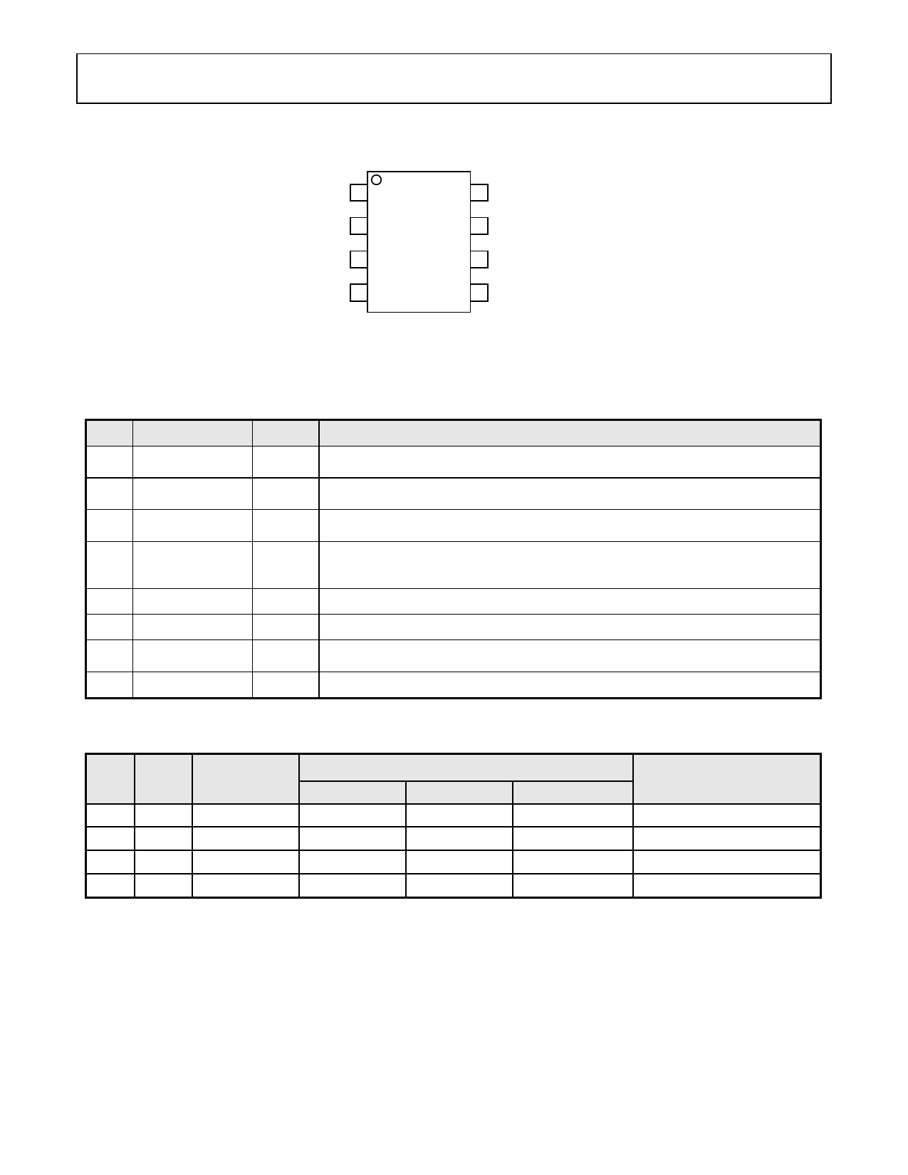
Pin Configuration
XIN / CLKIN 1
XOUT 2
FS1 3
LF 4
P278xA
8 VDD
7 FS0
6 ModOUT
5 VSS
Standard pin Configuration offered in both
8 pin SOIC Packages.
Pin Description (P278xA)
Pin# Pin Name
Type
1
XIN/CLKIN
I
2
XOUT
O
3
FS1
I
4
LF
I
5
VSS
I
6
ModOUT
O
7
FS0
I
8
VDD
P
Description
Connect to crystal or clock input. This pin has dual functions. It can be connected
either to an external crystal or an external reference clock.
Crystal connection. If using an external reference, this pin must be left
unconnected.
Digital logic input used to select input frequency range (see the Input Frequency
Selection Table). This pin has an internal pull-up resistor.
External Loop Filter for the PLL. By changing the value of the CRC circuit, the
percentage spread can be adjusted accordingly. See the Loop Filter Selection
Table for detail value.
Ground Connection. Connect to system ground.
Spread Spectrum Clock Output.
Digital logic input used to select input frequency range (see the Input Frequency
Selection Table). This pin has an internal pull-up resistor.
Connect to +3.3 V
Input Frequency Selection Table
FS1 FS0 Input (MHz)
Output Frequency Scaling (MHz)
P2781A
P2782A
P2784A
0
0
3 to 9
3 to 9
6 to 18
12 to 36
0
1
10 to 19
10 to 19
20 to 38
40 to 76
1
0
20 to 38
20 to 38
40 to 76
80 to 152
1
1
39 to 78
39 to 78
78 to 156
156 to 312
Modulation Rate (KHz)
Fin / 128
Fin / 256
Fin / 512
Fin / 1024
Rev. 2 | Page 2 of 8 | www.onsemi.com
Share Link: 