TDA4881 查看數據表(PDF) - Philips Electronics
零件编号
产品描述 (功能)
生产厂家
TDA4881 Datasheet PDF : 12 Pages
| |||
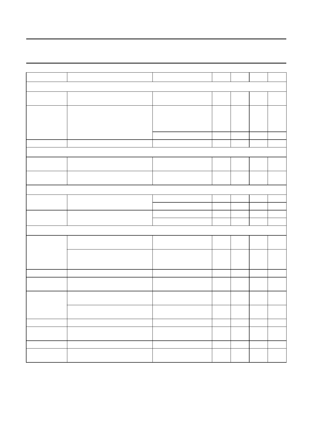
Philips Semiconductors
Advanced monitor video controller
Preliminary specification
TDA4881
SYMBOL
PARAMETER
CONDITIONS
MIN. TYP. MAX. UNIT
Voltage outputs (pins 19, 16 and 13)
VO(b-w)
signal output voltage
(black-to-white value)
Vbl
black level voltage
S/N
signal-to-noise ratio
Frequency response at voltage outputs
Gvf
gain decrease by frequency
response at pins 19, 16 and 13
trO
rise time at voltage output
(pins 19, 16 and 13)
V3, 11 open; V6 = 4.5 V; −
0.8 −
V
Vl(b-w) = 0.7 V
during output clamping; 0.3 −
1.0 V
depending on black
level adjustment;
see note 4
during switch-off
−
0.1 0.3 V
see note 5
−
−
44
dB
70 MHz
−
10% to 90% amplitude; −
input rise time = 1 ns
−
−3
dB
4.5 5.0 ns
Current outputs (pins 20, 17 and 14)
lO(b-w)
signal current (black-to-white)
V20-19, 17-16, 14-13 HF saturation of output transistors
−
with peaking; see note 6 −
IO = 50 mA
−
IO = 100 mA
−
Threshold voltages (see note 7)
V9
threshold for horizontal blanking
1.2
(blanking, output clamping)
threshold for switch-off
5.8
(blanking, minimum black level,
no output clamping)
R9
input resistance referenced to ground
50
td9
delay between horizontal blanking
−
input and output signal blanking
V10
threshold for vertical blanking
see Fig.4
1.2
(blanking, no input clamping)
threshold for clamping
see Fig.4
2.6
(input clamping, no blanking)
I10
input current
−3
tr,f10
rise and fall time for clamping pulse transition 1 to 3.5 V;
−
see Fig.4
tw10
clamping pulse width
V10 = 3 V
0.6
td10
delay between vertical blanking input see Fig.4
−
and output signal blanking
50
−
mA
−
100 mA
−
2.0 V
−
2.2 V
1.4 1.6 V
6.5 6.8 V
80
110 kΩ
35
60
ns
1.4 1.6 V
3.0 3.5 V
−1
−
µA
−
75
ns/V
−
−
µs
300 −
ns
November 1992
9
Share Link: 