M66260FP жҹҘзңӢж•ёж“ҡиЎЁпјҲPDFпјү - MITSUBISHI ELECTRIC
йӣ¶д»¶зј–еҸ·
дә§е“ҒжҸҸиҝ° (еҠҹиғҪ)
з”ҹдә§еҺӮ家
M66260FP Datasheet PDF : 6 Pages
| |||
MITMSUITBSIUSBHISвҢ©HDIGвҢ©DITIAGLITALSSAPSвҢӘSPвҢӘ
M662M66062F6P0FP
8 Г— 48 CГ— R4OCSRSOPSOSINPOT ISNWT ISTWCHITwCiHthwMitIhXMINIGXINFUGNFCUTNIOCNTION
DESCRIPTION
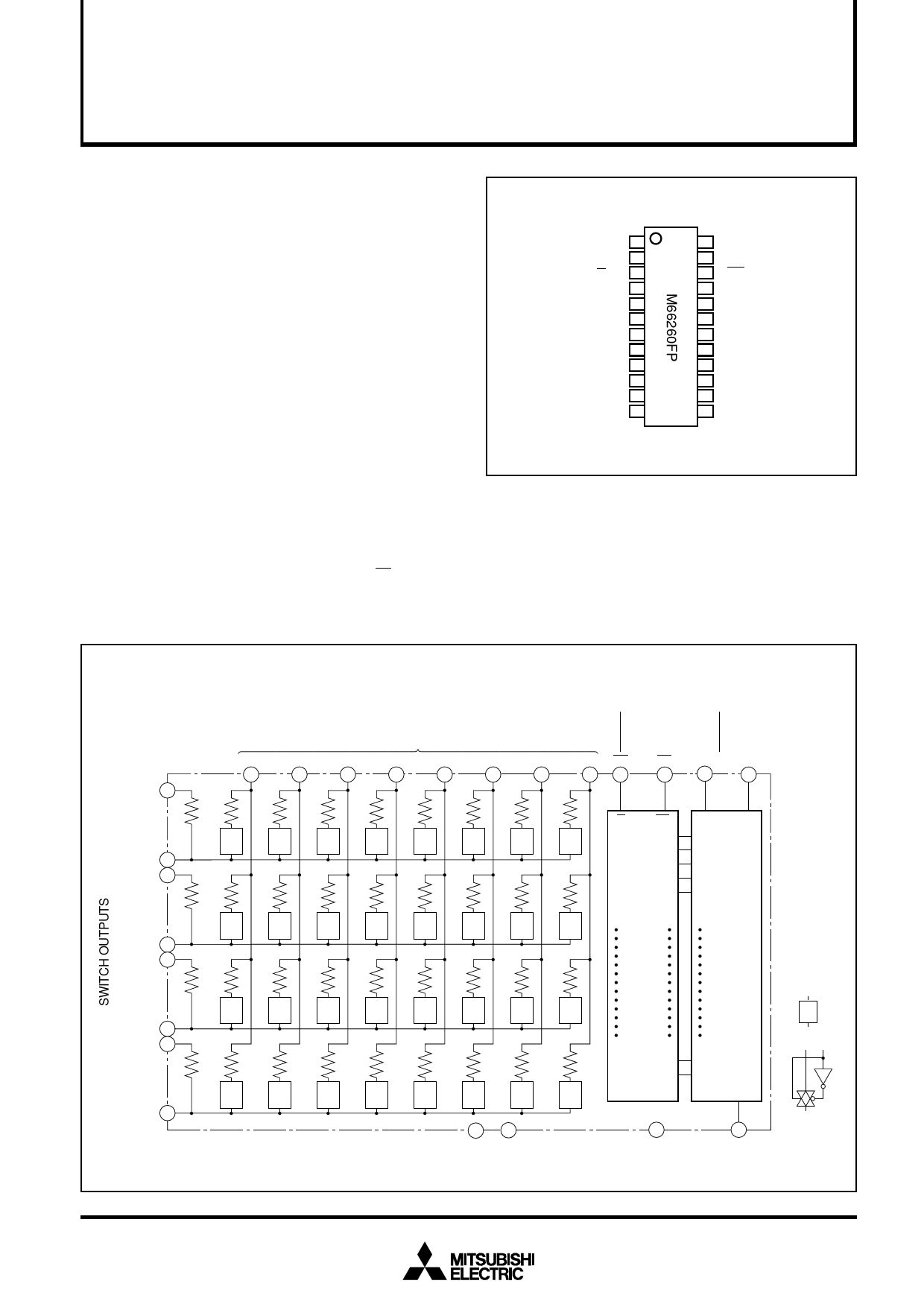
The M66260 is an integrated circuit consisiting of a 8 Г— 4
cross point switch capable of selecting 32 analog switches
with mixing registance respectively by serial control inputs.
Using the M66260 with an external standard Op-Amp, 8 ana-
log input signals can be mixed and output to any of 4 outputs
freely by serial control inputs.
FEATURES
вҖў Serial data input type
вҖў Switching and mixing function possible with standard Op-
Amp.
вҖў Switch matrix can be extended to 8 Г— 8 or 8 Г— 12 by com-
bining 2 or 3 ICs in parallel.
вҖў Excellent crosstalk characteristic
.......................... вҖ“90 dB [f = 3 kHz, VIN = вҖ“10dBV] (typ.)
APPLICATION
Line switching with mixing function of telephone and commu-
nication equipments.
FUNCTION
Serial data input A is the data input of the first step of 32 BIT
SHIFT REGISTER and when latch enable input LE is вҖңLвҖқ, the
signal of A shifts shifting registers one by one when shift
clock input CKs changes from вҖңLвҖқ to вҖңHвҖқ, in units of 32 bits.
PIN CONFIGURATION (TOP VIEW)
SHIFT CLOCK INPUT CKS вҶ’ 1
SHIFT DATA INPUT
AвҶ’ 2
DIRECT-CONNECTED
RESET INPUT
SWITCH INPUT
RD вҶ’ 3
пЈұпЈҙпЈІпЈҙпЈі
X0
X2
X4
X6
вҶ’
вҶ’
вҶ’
вҶ’
4
5
6
7
SWITCH
OUTPUT пЈұпЈҙпЈІпЈҙпЈіYYOOYYUUSSTT0101
вҶҗ
вҶҗ
вҶҗ
вҶҗ
8
9
10
11
GND 12
24 VCC
23 вҶ’SQ31 SHIFT DATA OUTPUT
22 вҶҗLE LATCH ENABLE INPUT
21
20
19
18
вҶҗвҶҗвҶҗвҶҗXXXX1357пЈјпЈҙпЈҪпЈҙпЈҫ
SWITCH INPUT
17
16
15
14
вҶ’
вҶ’
вҶ’
вҶ’
YOUT3
YS3
YS2
YOUT2
пЈјпЈҙпЈҪпЈҙпЈҫSWITCH
OUTPUT
13 VCC
Outline 24P2N-B
The 32 bits are stored into LATCH CIRCUIT in parallel when
latch enable LE changes from вҖңLвҖқ to вҖңHвҖқ.
Analog switches come on in a low-impedance state when
the output of the corresponding latch circuit is вҖңHвҖқ. They
come off in a high-impedance stage when the output of the
corresponding circuit is вҖңLвҖқ.
BLOCK DIAGRAM
DIRECT
RESET INPUT
SHIFT CLOCK
INPUT
пЈұ YOUT0 8
пЈҙ
пЈҙ
пЈҙ
пЈҙ
пЈҙ
пЈҙ
YS0
9
пЈҙ YOUT1 11
пЈҙ
пЈҙ
пЈҙ
пЈҙ
пЈҙ
пЈІ
пЈҙ
YS1
YOUT2
10
14
пЈҙ
пЈҙ
пЈҙ
пЈҙ
пЈҙ YS2 15
пЈҙ
пЈҙ
YOUT3
17
пЈҙ
пЈҙ
пЈҙ
пЈҙ
пЈі YS3 16
LATCH ENABLE SHIFT DATA
SWITCH INPUTS
INPUT
INPUT
X7
X6
X5
X4
X3
X2
X1
X0 RD LE CKS A
18
7
19
6
20
5
21
43
22 1
2
R LE CK DIN
7
6
5
4
3
2
1
0
QL0 DL0 QS0
QL1 DL1 QS1
QL2 DL2 QS2
QL3 DL3 QS3
QL4 DL4 QS4
15
14
13
12
11
10
9
8
23
22
21
20
19
18
17
16
LATCH
CIRCUIT
(Г— 32)
32-BIT
SHIFT
REGISTER
Note 1:
n
QLn
QL30 DL30 QS30
QL31 DL31 QS31
31
30
29
28
27
26
25
24
12 13
GND VCC
n = 0~31
24
23
VCC
SQ31
SHIFT DATA OUTPUT
1
Share Link: 