LF43881 查看數據表(PDF) - LOGIC Devices
零件编号
产品描述 (功能)
生产厂家
LF43881 Datasheet PDF : 11 Pages
| |||
DEVICES INCORPORATED
LF43881
8 x 8-bit Digital Filter
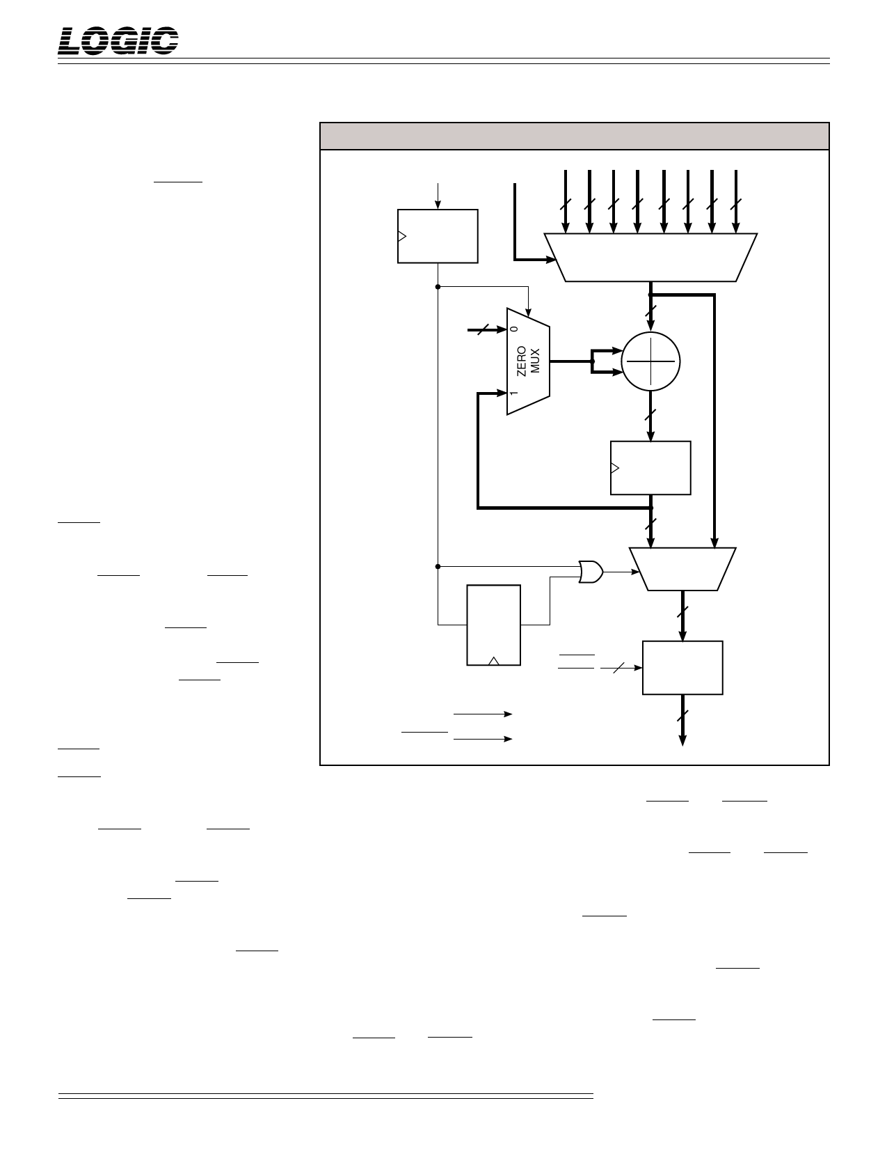
FILTER CELL DESCRIPTION
8-bit coefficients are loaded into the
C register (CIN7-0) and are output as
COUT7-0 (the COENB signal enables
the COUT7-0 outputs). The path
taken by the coefficients varies
according to the decimation mode
chosen. With no decimation, the
coefficients move directly from the
C register, bypassing all decimation
registers, and are available at the
output on the following clock cycle.
When decimation is chosen, the
coefficient output is delayed by 1, 2,
or 3 clock cycles depending on how
many decimation registers the
coefficients pass through (D1, D2, or
D3). The number of decimation
registers the coefficients pass
through is determined by DCM1-0.
Refer to Table 1 for choosing a
decimation mode.
CIENB enables the C and D registers
for coefficient loading. The registers
are loaded on the rising edge of CLK
when CIENB is LOW. CIENB is
latched and delayed internally which
enables the registers for loading one
clock cycle after CIENB goes active
(loading takes place on the second
rising edge of CLK after CIENB goes
LOW). Therefore, CIENB must be
LOW one clock cycle before the
coefficients are placed on the CIN7-0
inputs. The coefficients are held when
CIENB is HIGH.
FIGURE 2. OUTPUT STAGE DIAGRAM
SHADD
D
ADR2-0.D
26 26 26 26 26 26 26 26
Q
CELL RESULT
MUX
18
0
26
SIGN
EXTENSION
25-18
17-0
17-0
26
D
CLK
RESET.D
OUTPUT
BUFFER
25-8
26
1
0
OUTPUT
MUX
26
Q
SENBL 2
SENBH
TRI-STATE
BUFFER
TO ALL REGISTERS
26
TO ALL REGISTERS
DIENB enables the X register for the
loading of data. The X register is
loaded on the rising edge of CLK
when DIENB is LOW. DIENB is
latched and delayed internally (load-
ing takes place on the second rising
edge of CLK after DIENB goes LOW).
Therefore, DIENB must be LOW one
clock cycle before the data is placed on
the DIN7-0 inputs. The X register is
loaded with all zeros when DIENB is
HIGH.
The output of the C register (C8-0) and
X register (X8-0) provide the inputs of
the 8 x 8 multiplier. The multiplier is
followed by two pipeline registers,
M REG0 and M REG1. The output of
the multiplier is sign extended and is
used as one of the inputs to the 26-bit
adder. The output of the 26-bit
accumulator provides the second
input to the adder. Both the accumu-
lator and T register are loaded simul-
taneously with the output of the
adder.
The accumulator is loaded with the
output of the adder on every clock
cycle unless cleared. Clearing the
accumulator can be achieved using
two methods. The first method, when
both RESET and ERASE are LOW,
causes all accumulators and all
registers in the device to be cleared
together. RESET and ERASE are
latched and delayed internally caus-
ing the clearing to occur on the second
clock cycle after RESET and ERASE go
active.
The second method, when only
ERASE is LOW, clears a single accu-
mulator of a selected cell. The cell is
selected using the ADR2-0 inputs
(decoded to Cell n). ERASE is latched
and delayed internally causing the
clearing to occur on the second clock
cycle after ERASE goes active. Refer
to Table 2 for clearing registers and
accumulators.
Video Imaging Products
3
08/16/2000–LDS.43881-J
Share Link: 