LF43881 查看數據表(PDF) - LOGIC Devices
零件编号
产品描述 (功能)
生产厂家
LF43881 Datasheet PDF : 11 Pages
| |||
DEVICES INCORPORATED
LF43881
8 x 8-bit Digital Filter
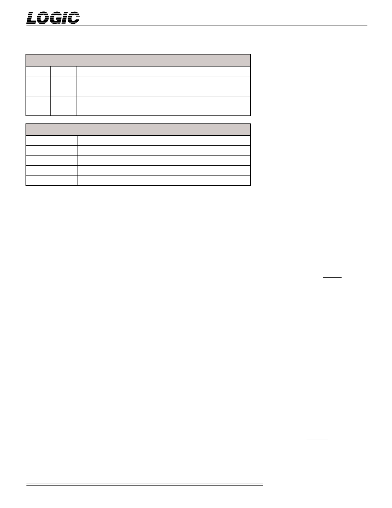
TABLE 1. DECIMATION MODE SELECTION
DCM1 DCM0 Decimation Function
0
0
Decimation registers not used
0
1
One decimation register used (decimation by one-half)
1
0
Two decimation registers used (decimation by one-third)
1
1
Three decimation registers used (decimation by one-fourth)
SIGNAL DEFINITIONS
Power
VCC and GND
+5 V power supply. All pins must be
connected.
Clock
TABLE 2. REGISTER AND ACCUMULATOR CLEARING
CLK — Master Clock
ERASE RESET
0
0
0
1
1
0
1
1
Clearing Effect
All accumulators and all registers are cleared
Only the accumulator addressed by ADR2-0 is cleared
All registers are cleared (accumulators are not cleared)
No clearing occurs, internal state remains the same
OUTPUT STAGE DESCRIPTION
The 26-bit adder contained in the
output stage can add the contents of
any filter cell accumulator (selected by
ADR2-0) with the 18 most significant
bits of the output buffer. The result is
stored back into the output buffer.
The complete operation takes only one
clock cycle. The eight least significant
bits of the output buffer are lost.
The Zero multiplexer is controlled by
the SHADD input signal. This allows
selection of either the 18 most signifi-
cant bits of the output buffer or all
zeros for the adder input. When
SHADD is LOW, all zeros will be
selected. When SHADD is HIGH, the
18 most significant bits of the output
buffer are selected enabling the shift-
and-add operation. SHADD is
latched and delayed internally by one
clock cycle.
The output multiplexer is also con-
trolled by the SHADD input signal.
This allows selection of either a filter
cell accumulator, selected by ADR2-0,
or the output buffer to be output to
the SUM25-0 bus. Only the 26 least
significant bits from either a filter cell
accumulator or the output buffer are
output on SUM25-0. If SHADD is
LOW during two consecutive clock
cycles (low during the current and
previous clock cycle), the output
multiplexer selects the contents of a
filter cell accumulator addressed by
ADR2-0. Otherwise, the output
multiplexer selects the contents of the
output buffer.
If the same address remains on the
ADR2-0 inputs for more than one clock
cycle, SUM25-0 will not change to
reflect any updates to the addressed
cell accumulator. Only the result from
the first selection of the cell (first clock
cycle) will be output. This allows the
interface of slow memory devices
where the output needs to be active
for more than one clock cycle. Normal
FIR operation is not affected because
ADR2-0 is changed sequentially.
NUMBER SYSTEMS
Data and coefficients can be repre-
sented as either unsigned or two's
complement numbers. The TCS and
TCCI inputs determine which of the
two formats is to be used. All values
are represented as 9-bit two's comple-
ment numbers internally. The value
of the ninth bit is determined by the
number system selected. The ninth bit
is a sign extended bit when the two's
complement mode is chosen. When
the unsigned mode is chosen, the
ninth bit is zero.
The rising edge of CLK strobes all
registers. All timing specifications are
referenced to the rising edge of CLK.
Inputs
DIN7-0 — Data Input
8-bit data is latched into the X register
of each filter cell simultaneously. The
TCS signal selects the appropriate
data format type. The DIENB signal
enables loading of the data.
CIN7-0 — Coefficient Input
8-bit coefficients are latched into the C
register of Filter Cell 0. The TCCI
signal selects the appropriate coeffi-
cient format type. The CIENB signal
enables loading of the coefficients.
Outputs
SUM25-0 — Data Output
The 26-bit result from an individual
filter cell will appear when ADR2-0 is
used to select the filter cell result.
SHADD in conjunction with ADR2-0 is
used to select the output from the
shift-and-add output stage.
COUT7-0 — Coefficient Output
The 8-bit coefficient output from
Filter Cell 7 can be connected to the
CIN7-0 coefficient input of the same
LF43881 to recirculate the coefficients.
COUT7-0 can also be connected to the
CIN7-0 of another LF43881 to cascade
the devices. The COENB signal
enables the output of the coefficients.
Video Imaging Products
4
08/16/2000–LDS.43881-J
Share Link: 