PIC16LC72-02/JW 查看數據表(PDF) - Microchip Technology
零件编号
产品描述 (功能)
生产厂家
PIC16LC72-02/JW Datasheet PDF : 124 Pages
| |||
2.0 MEMORY ORGANIZATION
There are two memory blocks in PIC16C72 Series
devices. These are the program memory and the data
memory. Each block has its own bus, so that access to
both blocks can occur during the same oscillator cycle.
The data memory can further be broken down into the
general purpose RAM and the Special Function
Registers (SFRs). The operation of the SFRs that
control the “core” are described here. The SFRs used
to control the peripheral modules are described in the
section discussing each individual peripheral module.
Additional information on device memory may be found
in the PICmicro™ Mid-Range Reference Manual,
DS33023.
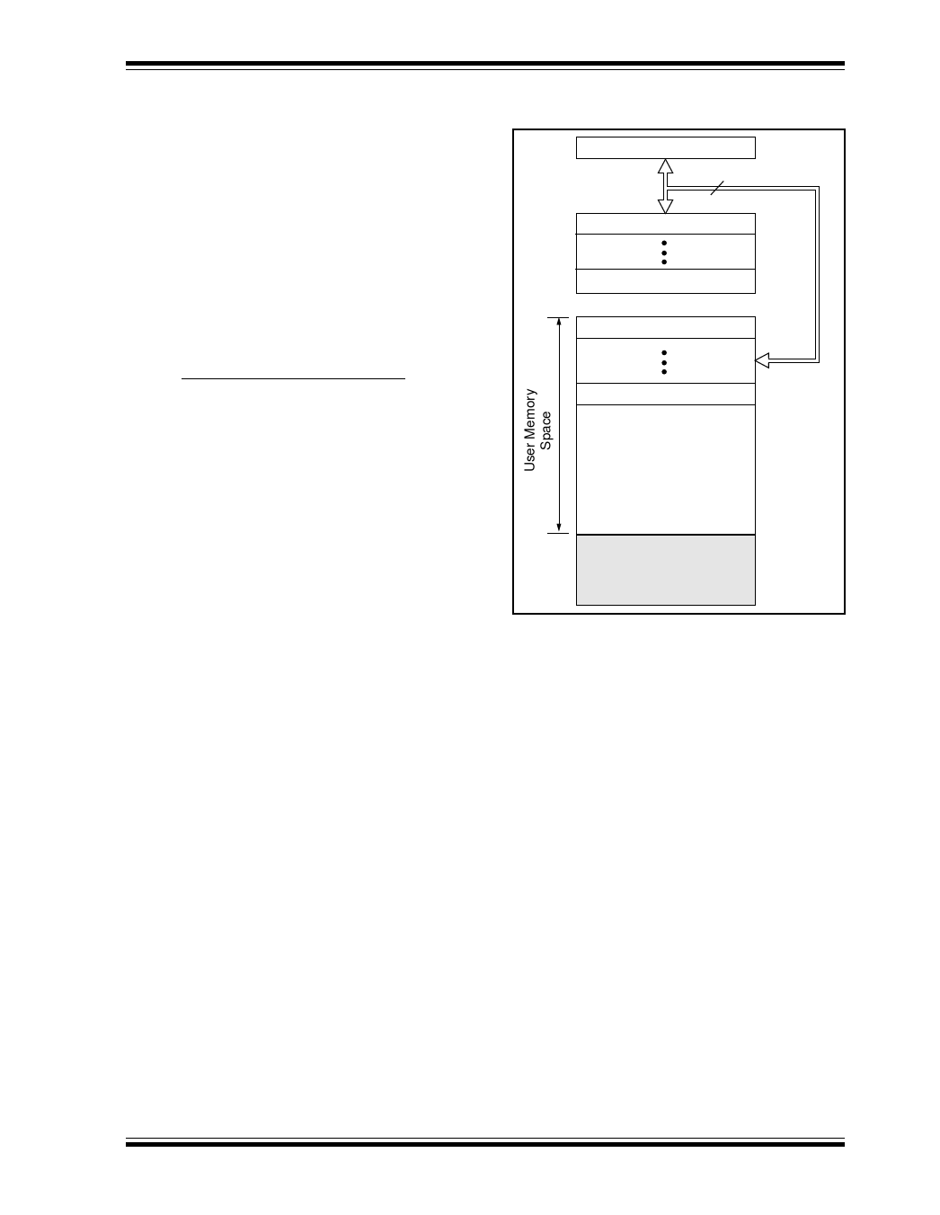
2.1 Program Memory Organization
PIC16C72 Series devices have a 13-bit program
counter capable of addressing a 2K x 14 program
memory space. The address range for this program
memory is 0000h - 07FFh. Accessing a location above
the physically implemented address will cause a wrap-
around.
The reset vector is at 0000h and the interrupt vector is
at 0004h.
PIC16C72 Series
FIGURE 2-1: PROGRAM MEMORY MAP
AND STACK
PC<12:0>
CALL, RETURN
RETFIE, RETLW
13
Stack Level 1
Stack Level 8
Reset Vector
0000h
Interrupt Vector
On-chip Program
Memory
0004h
0005h
07FFh
0800h
1FFFh
© 1998 Microchip Technology Inc.
Preliminary
DS39016A-page 5
Share Link: 