PCA8565 查看數據表(PDF) - Philips Electronics
零件编号
产品描述 (功能)
生产厂家
PCA8565 Datasheet PDF : 26 Pages
| |||
Philips Semiconductors
PCA8565
Real time clock/calender
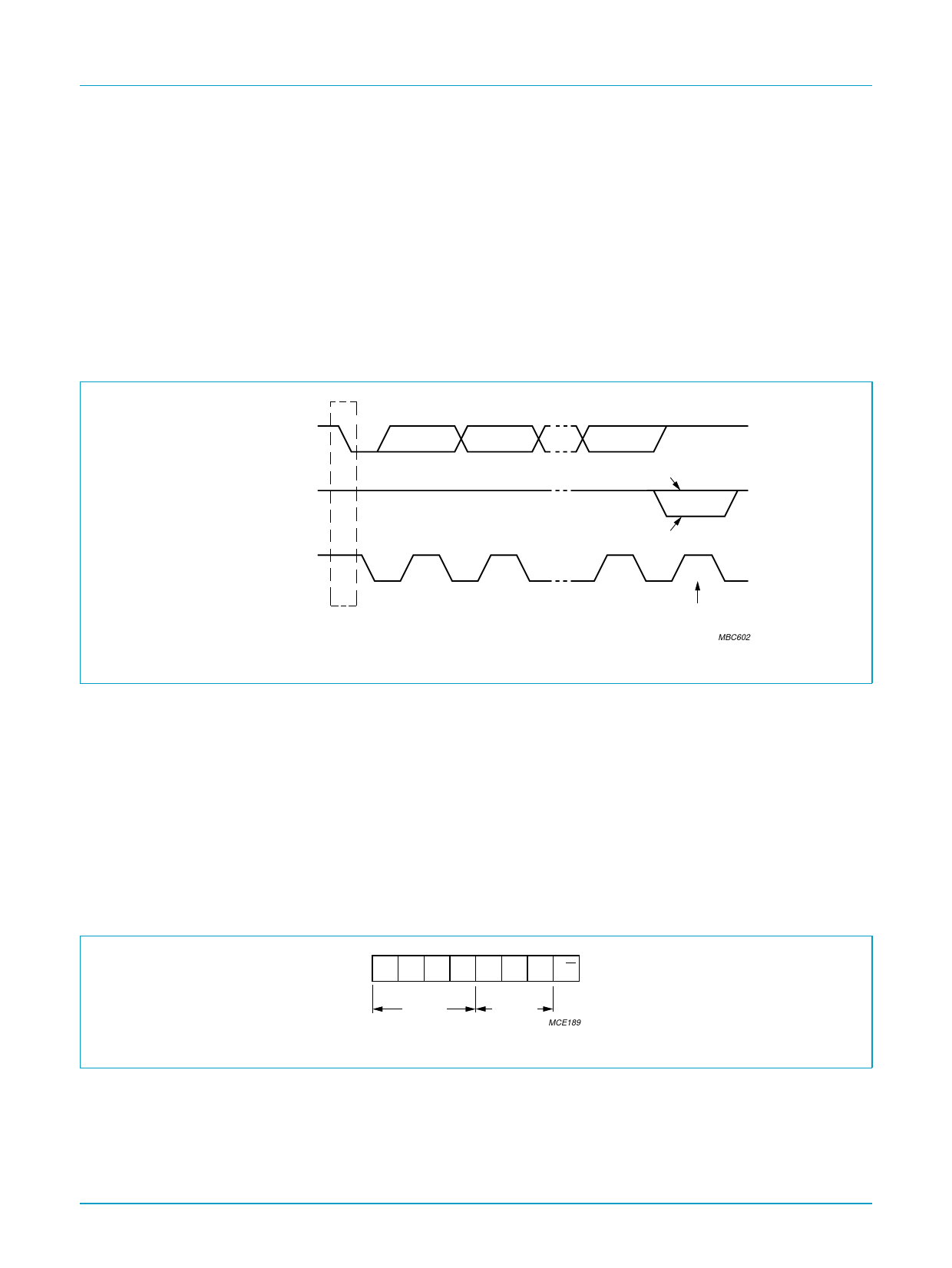
clock pulse. A slave receiver which is addressed must generate an acknowledge after
the reception of each byte. Also a master receiver must generate an acknowledge
after the reception of each byte that has been clocked out of the slave transmitter.
The device that acknowledges must pull down the SDA line during the acknowledge
clock pulse, so that the SDA line is stable LOW during the HIGH period of the
acknowledge related clock pulse (set-up and hold times must be taken into
consideration). A master receiver must signal an end of data to the transmitter by not
generating an acknowledge on the last byte that has been clocked out of the slave. In
this event the transmitter must leave the data line HIGH to enable the master to
generate a stop condition.
DATA OUTPUT
BY TRANSMITTER
DATA OUTPUT
BY RECEIVER
not acknowledge
acknowledge
SCL FROM
MASTER
1
2
S
START
condition
Fig 9. Acknowledgement on the I2C-bus.
8
9
clock pulse for
acknowledgement
MBC602
9.5 I2C-bus protocol
9.5.1 Addressing
Before any data is transmitted on the I2C-bus, the device which should respond is
addressed first. The addressing is always carried out with the first byte transmitted
after the start procedure.
The PCA8565 acts as a slave receiver or slave transmitter. Therefore the clock signal
SCL is only an input signal, but the data signal SDA is a bidirectional line.
The PCA8565 slave address is shown in Figure 10.
Fig 10. Slave address.
1 0 1 0 0 0 1 R/W
group 1
group 2
MCE189
9397 750 10695
Product data
Rev. 01 — 31 March 2003
© Koninklijke Philips Electronics N.V. 2003. All rights reserved.
13 of 26
Share Link: 