PCA9500 查看數據表(PDF) - Philips Electronics
零件编号
产品描述 (功能)
生产厂家
PCA9500 Datasheet PDF : 23 Pages
| |||
Philips Semiconductors
8-bit I2C and SMBus I/O port with 2-kbit EEPROM
Product data sheet
PCA9500
MEMORY OPERATIONS
Write operations
Write operations require an additional address field to indicate the
memory address location to be written. The address field is eight
bits long, providing access to any one of the 256 words of memory.
There are two types of write operations, byte write and page write.
Write operation is possible when WC control pin put at a low logic
level (0). When this control signal is set at 1, write operation is not
possible and data in the memory is protected.
Byte Write and Page Write explained below assume that Write
Control pin (WC) is set to 0.
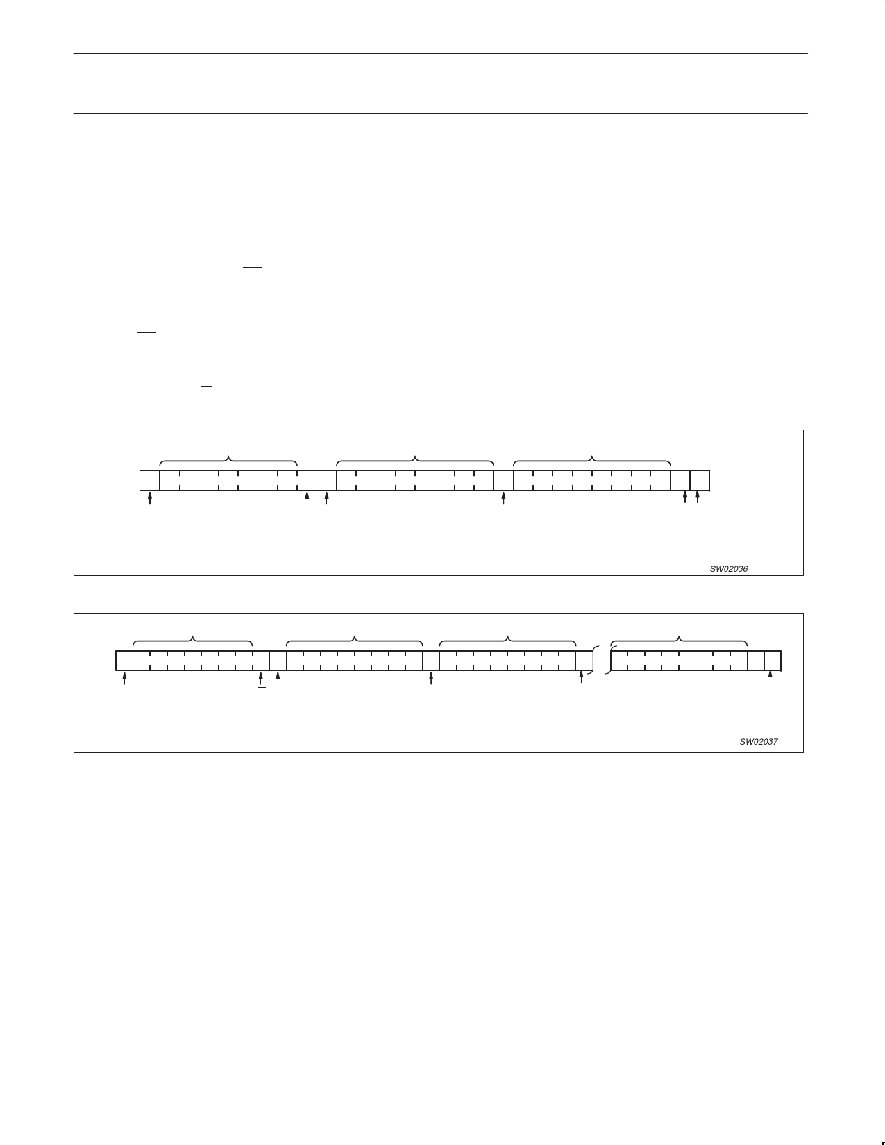
Byte Write (see Figure 9)
To perform a byte write the start condition is followed by the memory
slave address and the R/W bit set to 0. The PCA9500 will respond
with an acknowledge and then consider the next eight bits sent as
the word address and the eight bits after the word address as the
data. The PCA9500 will issue an acknowledge after the receipt of
both the word address and the data. To terminate the data transfer
the master issues the stop condition, initiating the internal write cycle
to the non-volatile memory. Only write and read operations to the
Quasi-bidirectional I/O are allowed during the internal write cycle.
Page Write (see Figure 10)
A page write is initiated in the same way as the byte write. If after
sending the first word of data, the stop condition is not received the
PCA9500 considers subsequent words as data. After each data
word the PCA9500 responds with an acknowledge and the two least
significant bits of the memory address field are incremented. Should
the master not send a stop condition after four data words the
address counter will return to its initial value and overwrite the data
previously written. After the receipt of the stop condition the inputs
will behave as with the byte write during the internal write cycle.
SLAVE ADDRESS (MEMORY)
WORD ADDRESS
DATA
SDA S 1 0 1 0 A2 A1 A0 0 A
A
DATA
AP
START CONDITION
R/W ACKNOWLEDGE
FROM SLAVE
ACKNOWLEDGE
FROM SLAVE
Figure 9. Byte write
ACKNOWLEDGE
FROM SLAVE
STOP CONDITION.
WRITE TO THE
MEMORY IS
PERFORMED
SW02036
SLAVE ADDRESS (MEMORY)
WORD ADDRESS
SDA S 1 0 1 0 A2 A1 A0 0 A
START CONDITION
R/W ACKNOWLEDGE
FROM SLAVE
DATA TO MEMORY
A
DATA n
A
ACKNOWLEDGE
FROM SLAVE
ACKNOWLEDGE
FROM SLAVE
Figure 10. Page Write
DATA TO MEMORY
DATA n + 3
AP
STOP CONDITION.
WRITE TO THE MEMORY
IS PERFORMED
SW02037
2004 Sep 30
7
Share Link: 