PCA9500 查看數據表(PDF) - NXP Semiconductors.
零件编号
产品描述 (功能)
生产厂家
PCA9500 Datasheet PDF : 26 Pages
| |||
NXP Semiconductors
PCA9500
8-bit I2C-bus and SMBus I/O port with 2-kbit EEPROM
7.3.1 Quasi-bidirectional I/Os
A quasi-bidirectional I/O can be used as an input or output without the use of a control
signal for data direction. At power-on the I/Os are HIGH. In this mode, only a current
source to VDD is active. An additional strong pull-up to VDD allows fast rising edges into
heavily loaded outputs. These devices turn on when an output is written HIGH, and are
switched off by the negative edge of SCL. The I/Os should be HIGH before being used as
inputs. See Figure 9.
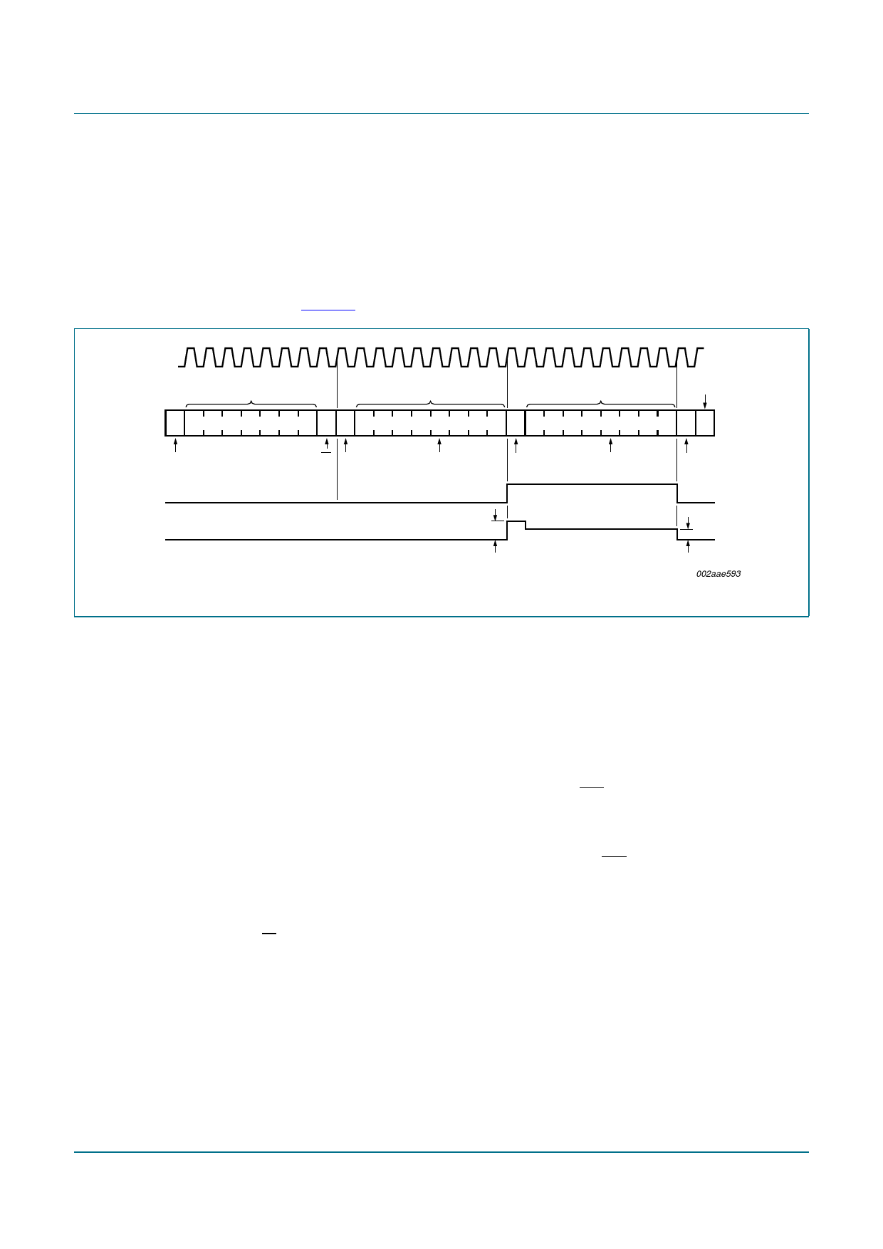
SCL 1 2 3 4 5 6 7 8 9
slave address (I/O expander)
data to port
data to port
STOP
condition
SDA S 0 1 0 0 A2 A1 A0 0 A
1
A
0
AP
START condition
IO3 output voltage
R/W acknowledge
IO3
from slave
acknowledge
IO3
from slave
acknowledge
from slave
IO3 pull-up output current
IOHt
IOH
002aae593
Fig 9. Transient pull-up current (IOHt) while IO3 changes from LOW to HIGH and back to LOW
7.4 Memory operations
7.4.1 Write operations
Write operations require an additional address field to indicate the memory address
location to be written. The address field is eight bits long, providing access to any one of
the 256 words of memory. There are two types of write operations, ‘byte write’ and
‘page write’.
Write operation is possible when the Write Control pin (WC) is put at a LOW logic level (0).
When this control signal is set at 1, write operation is not possible and data in the memory
is protected.
‘Byte write’ and ‘page write’ explained below assume that WC is set to 0.
7.4.1.1 Byte write
To perform a byte write the START condition is followed by the memory slave address and
the R/W bit set to 0. The PCA9500 will respond with an acknowledge and then consider
the next eight bits sent as the word address and the eight bits after the word address as
the data. The PCA9500 will issue an acknowledge after the receipt of both the word
address and the data. To terminate the data transfer the master issues the STOP
condition, initiating the internal write cycle to the non-volatile memory. Only write and read
operations to the quasi-bidirectional I/Os are allowed during the internal write cycle.
PCA9500_4
Product data sheet
Rev. 04 — 15 April 2009
© NXP B.V. 2009. All rights reserved.
7 of 26
Share Link: 