PCA9534D 查看數據表(PDF) - Philips Electronics
零件编号
产品描述 (功能)
生产厂家
PCA9534D Datasheet PDF : 17 Pages
| |||
Philips Semiconductors
8-bit I2C and SMBus low power I/O port with interrupt
Product data sheet
PCA9534
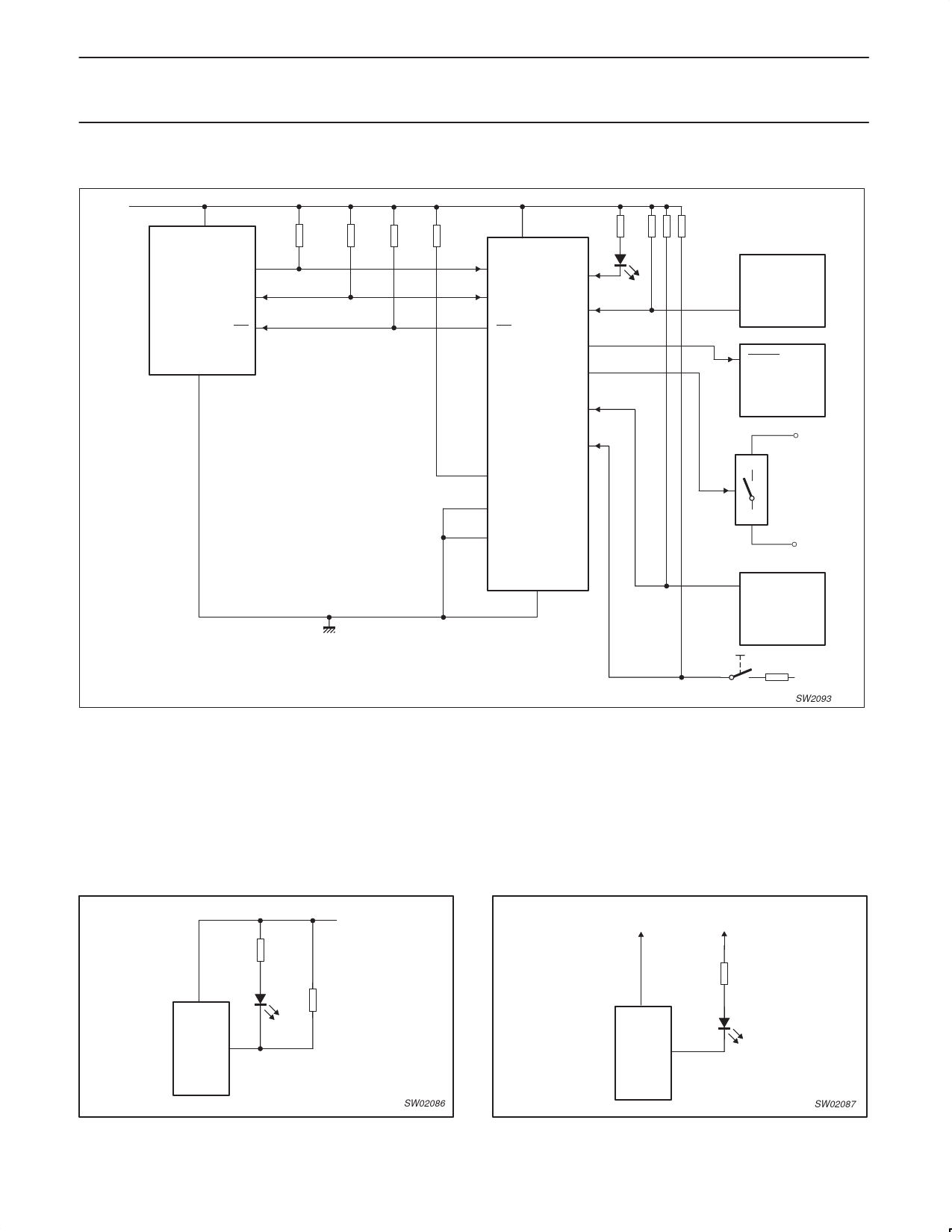
TYPICAL APPLICATION
VDD
(5 V)
VDD
10 kΩ
SCL
MASTER
CONTROLLER
SDA
INT
10 kΩ 10 kΩ 10 kΩ
GND
VDD
2 kΩ
I/O1
INT
I/O2
I/O3
PCA9534
I/O4
I/O5
A2
I/O6
A1
I/O7
A0
100 kΩ
(×3)
INT
RESET
SUBSYSTEM 2
(e.g. counter)
A
ENABLE
Controlled Switch
(e.g. CBT device)
B
VSS
ALARM
SUBSYSTEM 3
(e.g. alarm
system)
NOTE: Device address configured as 0100100 for this example
I/O0, I/O1, I/O2, configured as outputs
I/O3, I/O4, I/O5, configured as inputs
I/O06, I/O7, are not used and have to be configured as outputs
Figure 10. Typical application
VDD
SW2093
Minimizing IDD when the I/O is used to control LEDs
When the I/Os are used to control LEDs, they are normally connected to VDD through a resistor as shown in Figure 10. Since the LED acts as a
diode, when the LED is off the I/O VIN is about 1.2 V less than VDD. The supply current, IDD, increases as VIN becomes lower than VDD and is
specified as ∆IDD in the DC characteristics table.
Designs needing to minimize current consumption, such as battery power applications, should consider maintaining the I/O pins greater than or
equal to VDD when the LED is off. Figure 11 shows a high value resistor in parallel with the LED. Figure 12 shows VDD less than the LED supply
voltage by at least 1.2 V. Both of these methods maintain the I/O VIN at or above VDD and prevents additional supply current consumption when
the LED is off.
VDD
3.3 V
5V
VDD
LEDx
LED
100 kΩ
SW02086
Figure 11. High value resistor in parallel with the LED
2004 Sep 30
8
VDD
LEDx
LED
SW02087
Figure 12. Device supplied by a lower voltage
Share Link: 