9536 وں¥çœ‹و•¸و“ڑè،¨ï¼ˆPDF) - Philips Electronics
零ن»¶ç¼–هڈ·
ن؛§ه“پوڈڈè؟° (هٹں能)
ç”ںن؛§هژ‚ه®¶
9536 Datasheet PDF : 16 Pages
| |||
Philips Semiconductors
4-bit I2C and SMBus I/O port
Objective data sheet
PCA9536
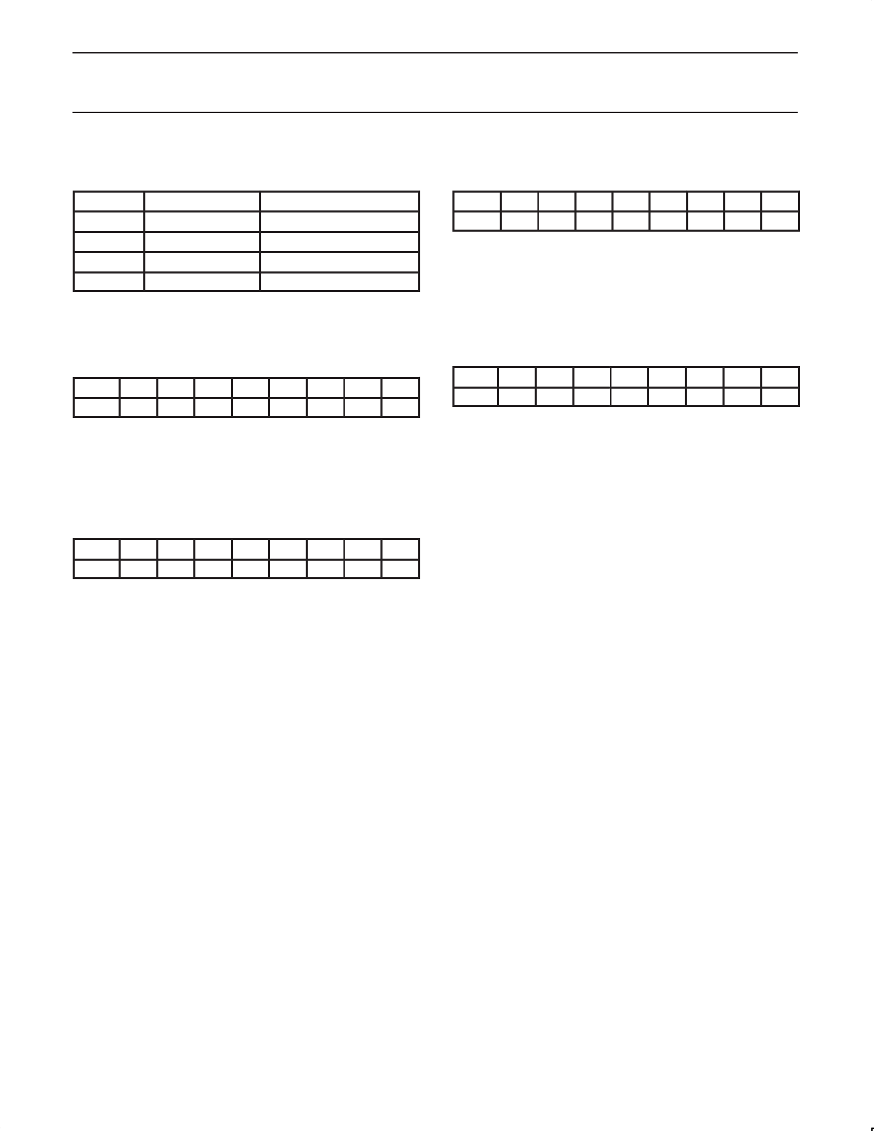
REGISTERS
Command Byte
Command
Protocol
Function
0
Read byte
Input port register
1
Read/write byte Output port register
2
Read/write byte Polarity inversion register
3
Read/write byte Configuration register
The command byte is the first byte to follow the address byte during
a write transmission. It is used as a pointer to determine which of the
following registers will be written or read.
Register 0 – Input Port Register
bit
X
X
X
X I3 I2 I1 I0
default 1
1
1
1
1
1
1
1
This register is a read only port. It reflects the incoming logic levels
of the pins, regardless of whether the pin is defined as an input or an
output by Register 3. Writes to this register have no effect.
“X†are “don’t care†bits and can be programmed with either “0â€
or “1â€.
Register 1 – Output Port Register
bit
X
X
X
X O3 O2 O1 O0
default 1
1
1
1
1
1
1
1
This register reflects the outgoing logic levels of the pins defined as
outputs by Register 3. Bit values in this register have no effect on
pins defined as inputs. Reads from this register return the value that
is in the flip-flop controlling the output selection, NOT the actual pin
value.
“X†are “don’t care†bits and can be programmed with either “0â€
or “1â€.
Register 2 – Polarity Inversion Register
bit
X
X
X
X N3 N2 N1 N0
default 0
0
0
0
0
0
0
0
This register allows the user to invert the polarity of the Input Port
Register data. If a bit in this register is set (written with â€ک1’), the
corresponding Input Port data is inverted. If a bit in this register is
cleared (written with a â€ک0’), the Input Port data polarity is retained.
“X†are “don’t care†bits and can be programmed with either “0â€
or “1â€.
Register 3 – Configuration Register
bit
X
X
X
X C3 C2 C1 C0
default 1
1
1
1
1
1
1
1
This register configures the directions of the I/O pins. If a bit in this
register is set, the corresponding port pin is enabled as an input with
high impedance output driver. If a bit in this register is cleared, the
corresponding port pin is enabled as an output. At reset, the I/Os are
configured as inputs with a weak pull-up to VDD.
“X†are “don’t care†bits and can be programmed with either “0â€
or “1â€.
Power-on Reset
When power is applied to VDD, an internal power-on reset holds the
PCA9536 in a reset condition until VDD has reached VPOR. At that
point, the reset condition is released and the PCA9536 registers and
state machine will initialize to their default states. Thereafter, VDD
must be lowered below 0.2 V to reset the device.
For a power reset cycle, VDD must be lowered below 0.2 V and then
restored to the operating voltage.
2004 Aug 20
4
Share Link: 