PCA9535A 查看數據表(PDF) - NXP Semiconductors.
零件编号
产品描述 (功能)
生产厂家
PCA9535A Datasheet PDF : 38 Pages
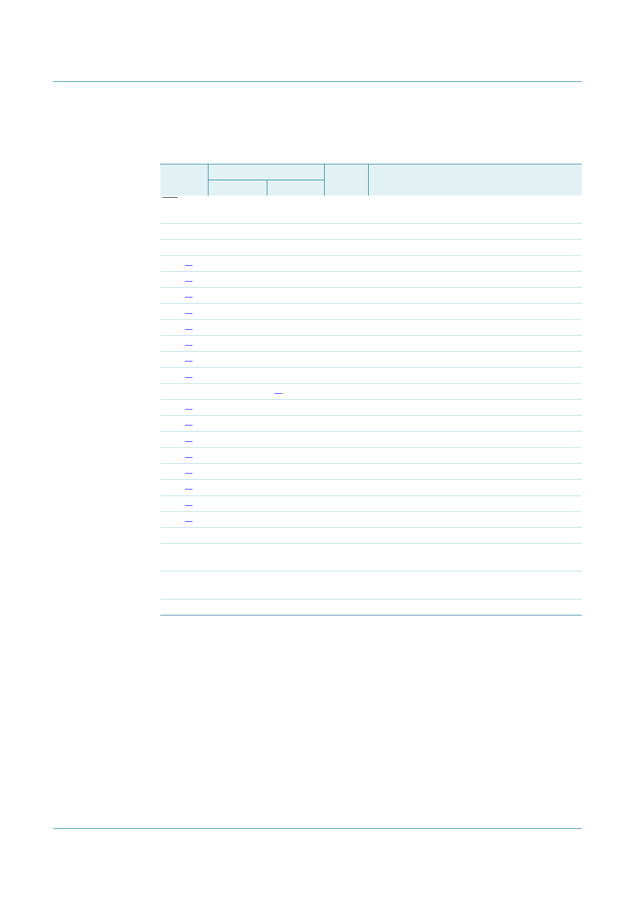
| |||
NXP Semiconductors
PCA9535A
Low-voltage 16-bit I2C-bus I/O port with interrupt
5.2 Pin description
Table 3.
Symbol
INT
Pin description
Pin
Type
TSSOP24 HWQFN24
1
22
O
A1
2
A2
3
P0_0[2] 4
P0_1[2] 5
P0_2[2] 6
P0_3[2] 7
P0_4[2] 8
P0_5[2] 9
P0_6[2] 10
P0_7[2] 11
VSS
12
P1_0[3] 13
P1_1[3] 14
P1_2[3] 15
P1_3[3] 16
P1_4[3] 17
P1_5[3] 18
P1_6[3] 19
P1_7[3] 20
A0
21
SCL
22
23
I
24
I
1
I/O
2
I/O
3
I/O
4
I/O
5
I/O
6
I/O
7
I/O
8
I/O
9[1]
power
10
I/O
11
I/O
12
I/O
13
I/O
14
I/O
15
I/O
16
I/O
17
I/O
18
I
19
I
SDA
23
20
I/O
VDD
24
21
power
Description
Interrupt output. Connect to VDD through a
pull-up resistor.
Address input 1. Connect directly to VDD or VSS.
Address input 2. Connect directly to VDD or VSS.
Port 0 input/output 0.
Port 0 input/output 1.
Port 0 input/output 2.
Port 0 input/output 3.
Port 0 input/output 4.
Port 0 input/output 5.
Port 0 input/output 6.
Port 0 input/output 7.
Ground.
Port 1 input/output 0.
Port 1 input/output 1.
Port 1 input/output 2.
Port 1 input/output 3.
Port 1 input/output 4.
Port 1 input/output 5.
Port 1 input/output 6.
Port 1 input/output 7.
Address input 0. Connect directly to VDD or VSS.
Serial clock bus. Connect to VDD through a
pull-up resistor.
Serial data bus. Connect to VDD through a
pull-up resistor.
Supply voltage.
[1] HWQFN24 package die supply ground is connected to both VSS pin and exposed center pad. VSS pin must
be connected to supply ground for proper device operation. For enhanced thermal, electrical, and board
level performance, the exposed pad needs to be soldered to the board using a corresponding thermal pad
on the board and for proper heat conduction through the board, thermal vias need to be incorporated in the
PCB in the thermal pad region.
[2] Pins P0_0 to P0_7 correspond to bits P0.0 to P0.7. At power-up, all I/O are configured as high-impedance
inputs.
[3] Pins P1_0 to P1_7 correspond to bits P1.0 to P1.7. At power-up, all I/O are configured as high-impedance
inputs.
PCA9535A
Product data sheet
All information provided in this document is subject to legal disclaimers.
Rev. 1 — 11 September 2012
© NXP B.V. 2012. All rights reserved.
4 of 38
Share Link: 