PCA9535A 查看數據表(PDF) - NXP Semiconductors.
零件编号
产品描述 (功能)
生产厂家
PCA9535A Datasheet PDF : 38 Pages
| |||
NXP Semiconductors
PCA9535A
Low-voltage 16-bit I2C-bus I/O port with interrupt
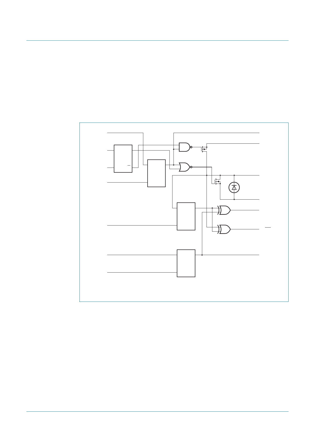
6.3 I/O port
When an I/O is configured as an input, FETs Q1 and Q2 are off, which creates a
high-impedance input. The input voltage may be raised above VDD to a maximum of 5.5 V.
If the I/O is configured as an output, Q1 or Q2 is enabled, depending on the state of the
Output port register. In this case, there are low-impedance paths between the I/O pin and
either VDD or VSS. The external voltage applied to this I/O pin should not exceed the
recommended levels for proper operation.
data from
shift register
data from
shift register
write
configuration
pulse
configuration
register
DQ
FF
CK Q
write pulse
read pulse
data from
shift register
write polarity
pulse
DQ
FF
CK
output port
register
input port
register
DQ
FF
CK
polarity
inversion
register
DQ
FF
CK
Q1
Q2
output port
register data
VDD
ESD
protection
diode
P0_0 to P0_7
P1_0 to P1_7
VSS
input port
register data
to INT
polarity
inversion
register data
002aah246
At power-on reset, all registers return to default values.
Fig 6. Simplified schematic of the I/Os (P0_0 to P0_7, P1_0 to P1_7)
PCA9535A
Product data sheet
All information provided in this document is subject to legal disclaimers.
Rev. 1 — 11 September 2012
© NXP B.V. 2012. All rights reserved.
8 of 38
Share Link: 