PCA9555A 查看數據表(PDF) - NXP Semiconductors.
零件编号
产品描述 (功能)
生产厂家
PCA9555A Datasheet PDF : 39 Pages
| |||
NXP Semiconductors
PCA9555A
Low-voltage 16-bit I2C-bus I/O port with interrupt and weak pull-up
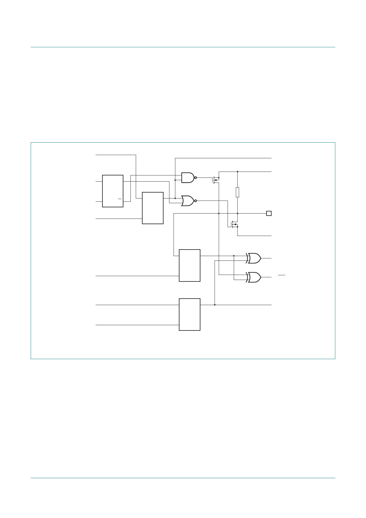
6.3 I/O port
When an I/O is configured as an input, FETs Q1 and Q2 are off, which creates a
high-impedance input. The input voltage may be raised above VDD to a maximum of 5.5 V.
If the I/O is configured as an output, Q1 or Q2 is enabled, depending on the state of the
Output port register. In this case, there are low-impedance paths between the I/O pin and
either VDD or VSS. The external voltage applied to this I/O pin should not exceed the
recommended levels for proper operation.
data from
shift register
data from
shift register
write configuration
pulse
configuration
register
D
Q
FF
CK Q
write pulse
D
Q
FF
CK
output port
register
read pulse
data from
shift register
write polarity
pulse
Q1
100 kΩ
Q2
input port
register
D
Q
FF
CK
polarity inversion
register
D
Q
FF
CK
At power-on reset, all registers return to default values.
Fig 6. Simplified schematic of the I/Os (P0_0 to P0_7, P1_0 to P1_7)
output port
register data
VDD
P0_0 to P0_7
P1_0 to P1_7
VSS
input port
register data
to INT
polarity inversion
register data
002aah328
PCA9555A
Product data sheet
All information provided in this document is subject to legal disclaimers.
Rev. 1 — 11 September 2012
© NXP B.V. 2012. All rights reserved.
8 of 39
Share Link: 