PCA9555D 查看數據表(PDF) - Philips Electronics
零件编号
产品描述 (功能)
生产厂家
PCA9555D Datasheet PDF : 22 Pages
| |||
Philips Semiconductors
16-bit I2C and SMBus I/O port with interrupt
Product data sheet
PCA9555
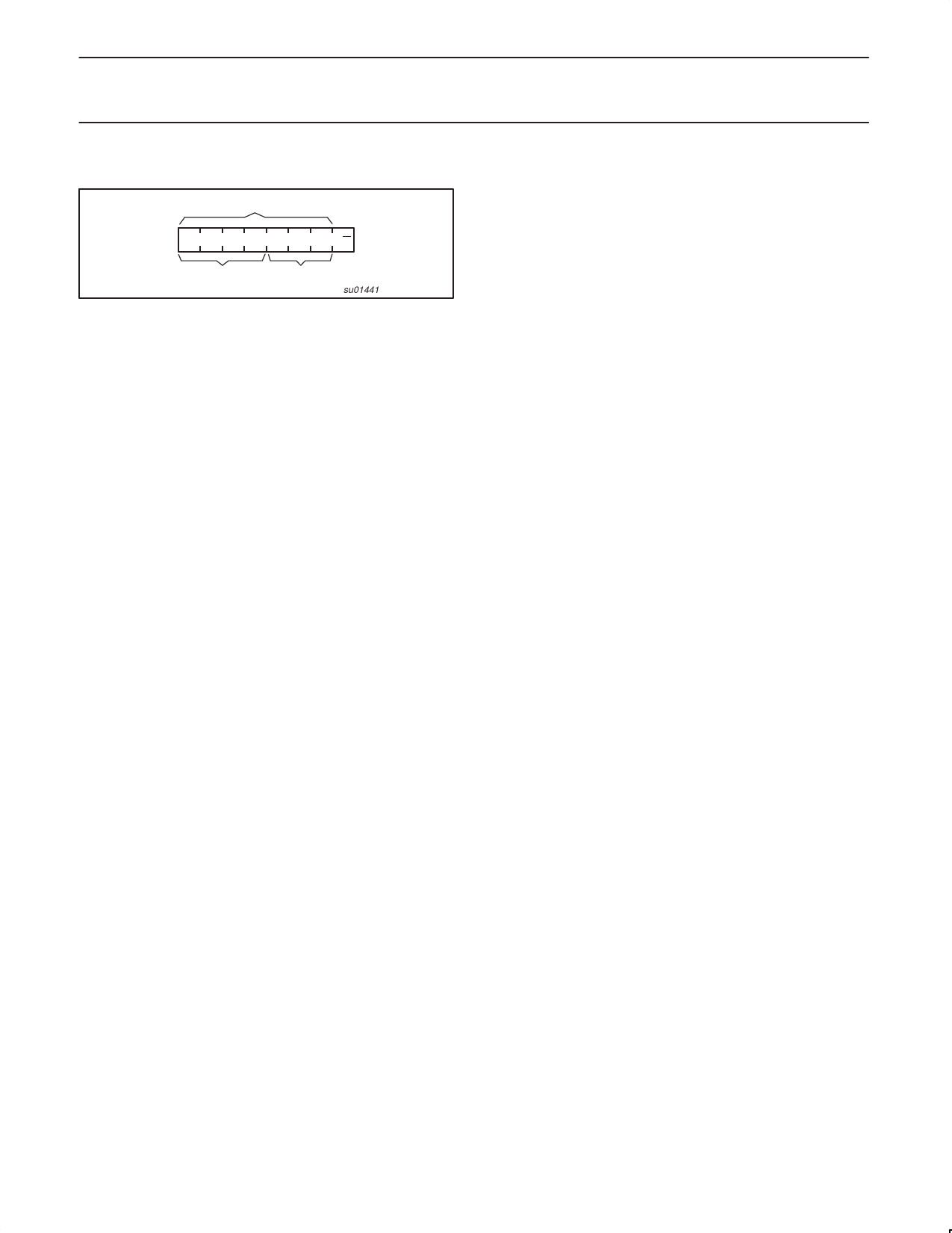
DEVICE ADDRESS
slave address
0 1 0 0 A2 A1 A0 R/W
fixed
programmable
su01441
Figure 5. PCA9555 address
BUS TRANSACTIONS
Writing to the port registers
Data is transmitted to the PCA9555 by sending the device address
and setting the least significant bit to a logic 0 (see Figure 5 for device
address). The command byte is sent after the address and determines
which register will receive the data following the command byte.
The eight registers within the PCA9555 are configured to operate
as four register pairs. The four pairs are Input Ports, Output Ports,
Polarity Inversion Ports, and Configuration Ports. After sending data
to one register, the next data byte will be sent to the other register in
the pair (see Figures and ). For example, if the first byte is sent to
Output Port (register 3), then the next byte will be stored in Output
Port 0 (register 2). There is no limitation on the number of data bytes
sent in one write transmission. In this way, each 8-bit register may
be updated independently of the other registers.
Reading the port registers
In order to read data from the PCA9555, the bus master must first
send the PCA9555 address with the least significant bit set to a
logic 0 (see Figure 5 for device address). The command byte is sent
after the address and determines which register will be accessed.
After a restart, the device address is sent again but this time, the
least significant bit is set to a logic 1. Data from the register defined
by the command byte will then be sent by the PCA9555 (see
Figures 8 and 9). Data is clocked into the register on the falling edge
of the acknowledge clock pulse. After the first byte is read, additional
bytes may be read but the data will now reflect the information in the
other register in the pair. For example, if you read Input Port 1, then
the next byte read would be Input Port 0. There is no limitation on
the number of data bytes received in one read transmission but the
final byte received, the bus master must not acknowledge the data.
Interrupt Output
The open-drain interrupt output is activated when one of the port
pins change state and the pin is configured as an input. The interrupt
is deactivated when the input returns to its previous state or the
input port register is read (see Figure 9). A pin configured as an
output cannot cause an interrupt. Since each 8-bit port is read
independently, the interrupt caused by Port 0 will not be cleared by a
read of Port 1 or the other way around.
Note that changing an I/O from an output to an input may cause a
false interrupt to occur if the state of the pin does not match the
contents of the Input Port register.
2004 Sep 30
7
Share Link: 