PCA9555 查看數據表(PDF) - NXP Semiconductors.
零件编号
产品描述 (功能)
生产厂家
PCA9555 Datasheet PDF : 34 Pages
| |||
NXP Semiconductors
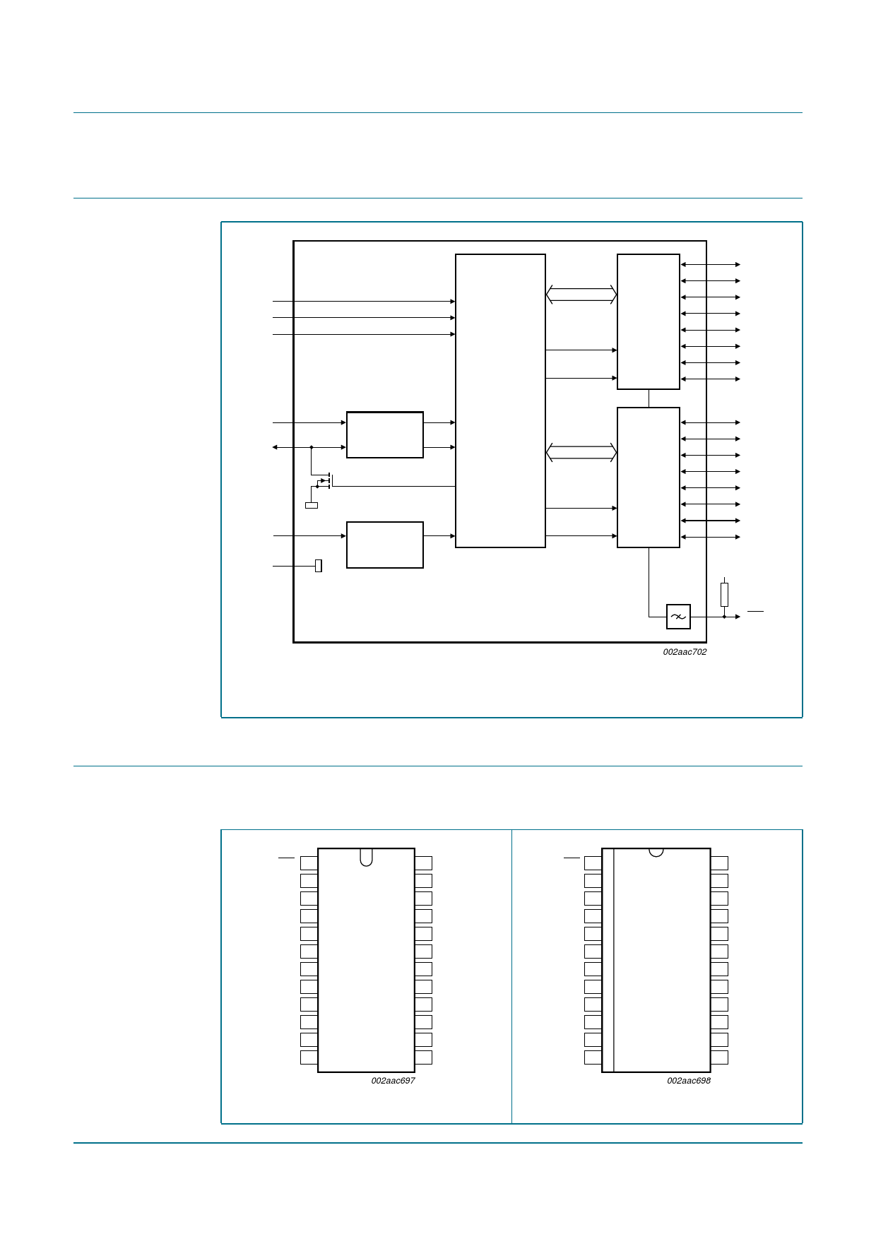
4. Block diagram
PCA9555
16-bit I2C-bus and SMBus I/O port with interrupt
PCA9555
A0
A1
A2
SCL
SDA
INPUT
FILTER
VDD
VSS
POWER-ON
RESET
8-bit
write pulse
I2C-BUS/SMBus
CONTROL
read pulse
INPUT/
OUTPUT
PORTS
8-bit
write pulse
read pulse
INPUT/
OUTPUT
PORTS
IO1_0
IO1_1
IO1_2
IO1_3
IO1_4
IO1_5
IO1_6
IO1_7
IO0_0
IO0_1
IO0_2
IO0_3
IO0_4
IO0_5
IO0_6
IO0_7
VDD
LP filter
INT
Remark: All I/Os are set to inputs at reset.
Fig 1. Block diagram of PCA9555
002aac702
5. Pinning information
5.1 Pinning
PCA9555_8
Product data sheet
INT 1
A1 2
A2 3
IO0_0 4
IO0_1 5
IO0_2 6
IO0_3 7
IO0_4 8
IO0_5 9
IO0_6 10
IO0_7 11
VSS 12
PCA9555N
24 VDD
23 SDA
22 SCL
21 A0
20 IO1_7
19 IO1_6
18 IO1_5
17 IO1_4
16 IO1_3
15 IO1_2
14 IO1_1
13 IO1_0
002aac697
INT 1
A1 2
A2 3
IO0_0 4
IO0_1 5
IO0_2 6
IO0_3 7
IO0_4 8
IO0_5 9
IO0_6 10
IO0_7 11
VSS 12
PCA9555D
24 VDD
23 SDA
22 SCL
21 A0
20 IO1_7
19 IO1_6
18 IO1_5
17 IO1_4
16 IO1_3
15 IO1_2
14 IO1_1
13 IO1_0
002aac698
Fig 2. Pin configuration for DIP24
Fig 3. Pin configuration for SO24
Rev. 08 — 22 October 2009
© NXP B.V. 2009. All rights reserved.
3 of 34
Share Link: 