PCA9555 查看數據表(PDF) - NXP Semiconductors.
零件编号
产品描述 (功能)
生产厂家
PCA9555 Datasheet PDF : 34 Pages
| |||
NXP Semiconductors
PCA9555
16-bit I2C-bus and SMBus I/O port with interrupt
6.2.5 Registers 6 and 7: Configuration registers
This register configures the directions of the I/O pins. If a bit in this register is set (written
with ‘1’), the corresponding port pin is enabled as an input with high-impedance output
driver. If a bit in this register is cleared (written with ‘0’), the corresponding port pin is
enabled as an output. Note that there is a high value resistor tied to VDD at each pin. At
reset, the device's ports are inputs with a pull-up to VDD.
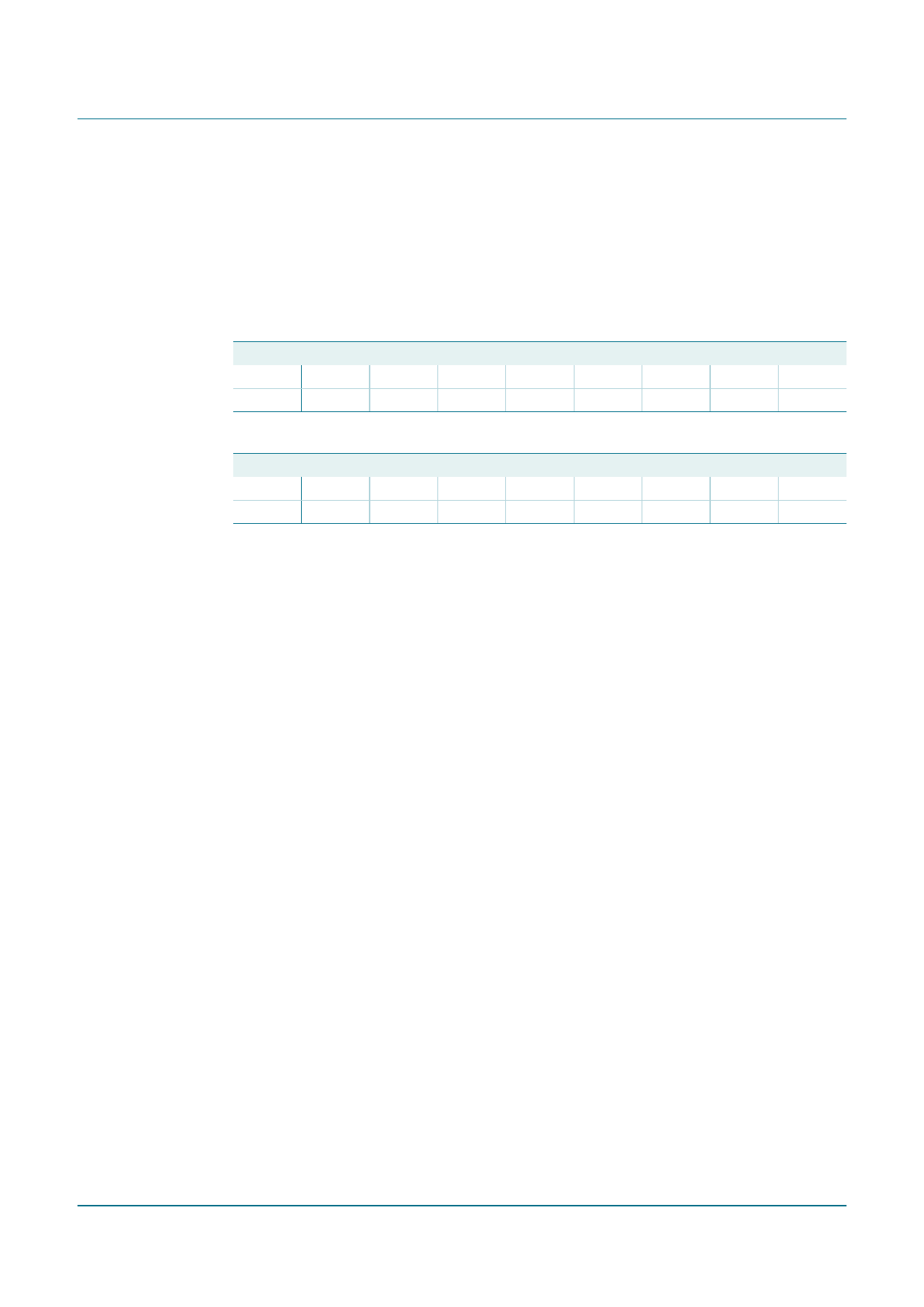
Table 11.
Bit
Symbol
Default
Configuration port 0 register
7
6
5
C0.7
C0.6
C0.5
1
1
1
4
C0.4
1
3
C0.3
1
2
C0.2
1
1
C0.1
1
0
C0.0
1
Table 12.
Bit
Symbol
Default
Configuration port 1 register
7
6
5
C1.7
C1.6
C1.5
1
1
1
4
C1.4
1
3
C1.3
1
2
C1.2
1
1
C1.1
1
0
C1.0
1
6.3 Power-on reset
When power is applied to VDD, an internal power-on reset holds the PCA9555 in a reset
condition until VDD has reached VPOR. At that point, the reset condition is released and the
PCA9555 registers and SMBus state machine will initialize to their default states. The
power-on reset typically completes the reset and enables the part by the time the power
supply is above VPOR. However, when it is required to reset the part by lowering the power
supply, it is necessary to lower it below 0.2 V.
6.4 I/O port
When an I/O is configured as an input, FETs Q1 and Q2 are off, creating a
high-impedance input with a weak pull-up to VDD. The input voltage may be raised above
VDD to a maximum of 5.5 V.
If the I/O is configured as an output, then either Q1 or Q2 is on, depending on the state of
the Output Port register. Care should be exercised if an external voltage is applied to an
I/O configured as an output because of the low-impedance path that exists between the
pin and either VDD or VSS.
PCA9555_8
Product data sheet
Rev. 08 — 22 October 2009
© NXP B.V. 2009. All rights reserved.
8 of 34
Share Link: 