PCA9555 查看數據表(PDF) - NXP Semiconductors.
零件编号
产品描述 (功能)
生产厂家
PCA9555 Datasheet PDF : 34 Pages
| |||
NXP Semiconductors
PCA9555
16-bit I2C-bus and SMBus I/O port with interrupt
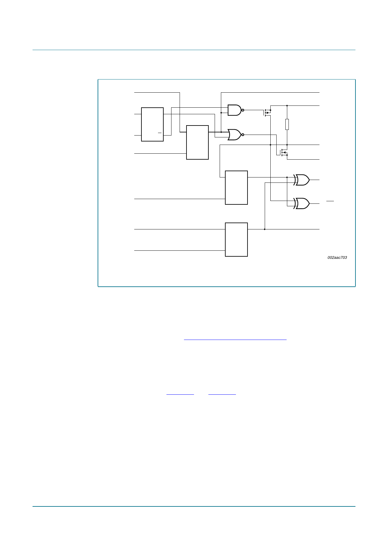
data from
shift register
data from
shift register
write
configuration
pulse
configuration
register
DQ
FF
CK Q
write pulse
read pulse
data from
shift register
write polarity
pulse
DQ
FF
CK
output port
register
Q1
100 kΩ
Q2
input port
register
DQ
FF
CK
polarity inversion
register
DQ
FF
CK
At power-on reset, all registers return to default values.
Fig 9. Simplified schematic of I/Os
output port
register data
VDD
I/O pin
VSS
input port
register data
to INT
polarity
inversion
register data
002aac703
6.5 Bus transactions
6.5.1 Writing to the port registers
Data is transmitted to the PCA9555 by sending the device address and setting the least
significant bit to a logic 0 (see Figure 8 “PCA9555 device address”). The command byte is
sent after the address and determines which register will receive the data following the
command byte.
The eight registers within the PCA9555 are configured to operate as four register pairs.
The four pairs are Input Ports, Output Ports, Polarity Inversion Ports, and Configuration
Ports. After sending data to one register, the next data byte will be sent to the other
register in the pair (see Figure 10 and Figure 11). For example, if the first byte is sent to
Output Port 1 (register 3), then the next byte will be stored in Output Port 0 (register 2).
There is no limitation on the number of data bytes sent in one write transmission. In this
way, each 8-bit register may be updated independently of the other registers.
PCA9555_8
Product data sheet
Rev. 08 — 22 October 2009
© NXP B.V. 2009. All rights reserved.
9 of 34
Share Link: 