PCF2105MU2 查看數據表(PDF) - Philips Electronics
零件编号
产品描述 (功能)
生产厂家
PCF2105MU2 Datasheet PDF : 48 Pages
| |||
Philips Semiconductors
LCD controller/driver
Product specification
PCF2105
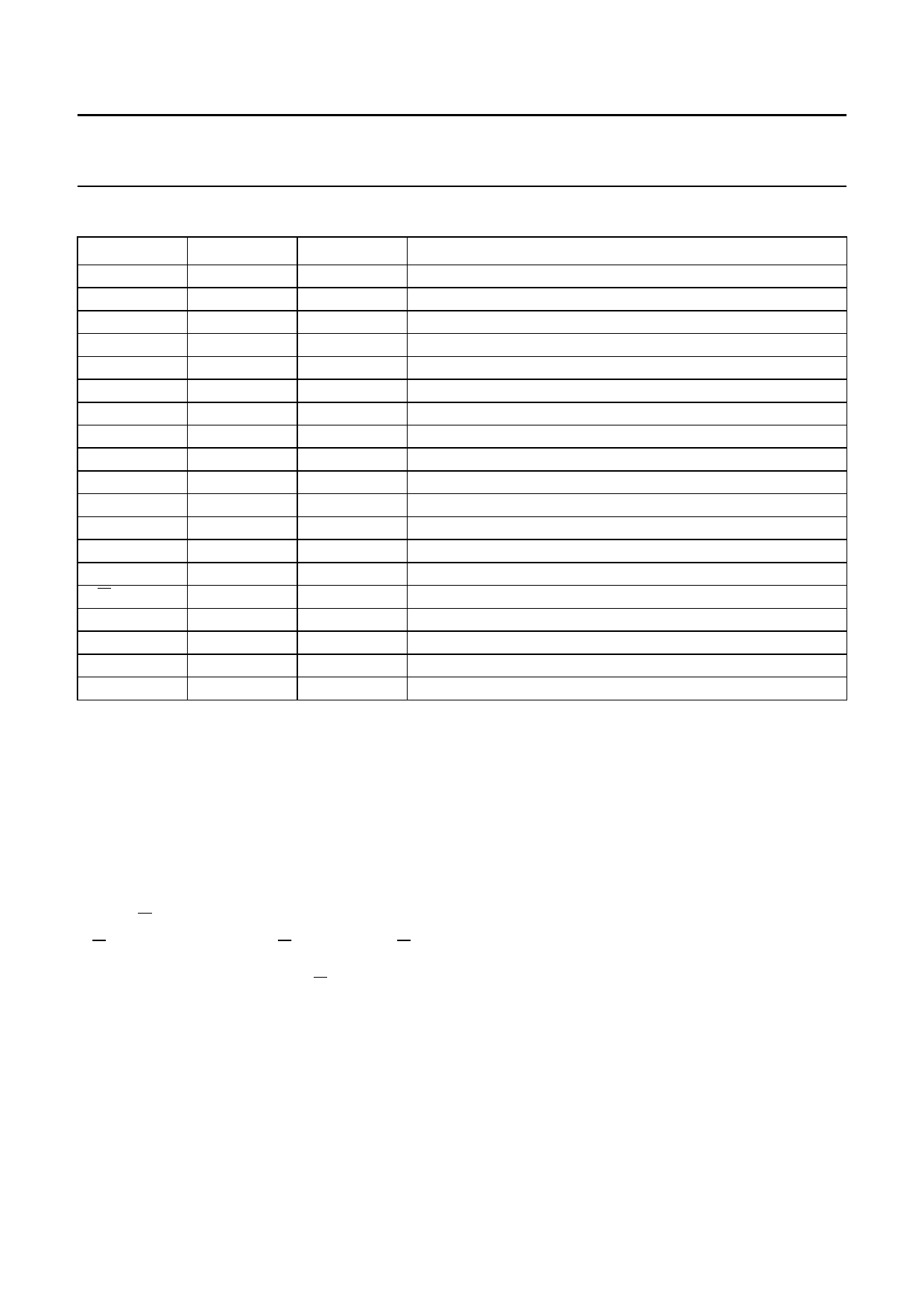
6 PINNING
SYMBOL
OSC
VDD
SA0
VSS
R8 to R5
R32 to R29
R24 to R17
C60 to C1
R9 to R16
R25 to R28
R1 to R4
SCL
E
RS
R/W
T1
DB7 to DB0
SDA
VLCD
PAD
1
2
3
4
5 to 8
9 to 12
13 to 20
21 to 80
81 to 88
89 to 92
93 to 96
97
98
99
100
101
102 to 109
110
111
I/O
DESCRIPTION
I
oscillator/external clock input
−
logic supply voltage
I
I2C-bus address selection input
−
logic ground
O
LCD row driver outputs
O
LCD row driver outputs
O
LCD row driver outputs
O
LCD column driver outputs
O
LCD row driver outputs
O
LCD row driver outputs
O
LCD row driver outputs
I
I2C-bus serial clock input
I
data bus clock input
I
register select input
I
read/write input
I
test input
I/O
8-bit bidirectional data bus input/output
I/O
I2C-bus serial data input/output
I
LCD supply voltage input
7 PAD FUNCTIONS
7.1 RS: Register Select (parallel control)
Bit RS selects the register to be accessed for read and
write when the device is controlled by the parallel interface.
RS = 0 selects the instruction register for write and the
busy flag and address counter for read. RS = 1 selects the
data register for both read and write. There is an internal
pull-up resistor on pad RS.
7.2 R/W: read/write (parallel control)
R/W selects either the read (R/W = 1) or write (R/W = 0)
operation when control is by the parallel interface. There is
an internal pull-up resistor on pad R/W.
7.3 E: data bus clock (parallel control)
Pad E should be HIGH to signal the start of a read or write
operation when the device is controlled by the parallel
interface. Data is clocked in or out of the chip on the falling
edge of the clock. Note that pad E must be connected to
VSS (logic 0) when I2C-bus control is used.
7.4 DB7 to DB0: data bus (parallel control)
The bidirectional, 3-state data bus transfers data between
the system controller and the PCF2105. DB7 acts as the
busy flag, signalling that internal operations are not yet
completed. In 4-bit operations, DB7 to DB4 are used and
DB3 to DB0 must be left open-circuit. There is an internal
pull-up resistor on each of the data lines. Note that
pads DB7 to DB0 must be left open-circuit when I2C-bus
control is used.
7.5 C60 to C1: column driver outputs
Pads C60 to C1 output the data for pairs of columns.
This arrangement permits optimized Chip-On-Glass
(COG) layout for 4-line by 12 characters.
7.6 R32 to R1: row driver outputs
Pads R32 to R1 output the row select waveforms to the
left and right halves of the display.
7.7 VLCD: LCD power supply
Negative power supply for the liquid crystal display.
1998 Jul 30
5
Share Link: 