42551-51 ТЪЦуюІТЋИТЊџУАе№╝ѕPDF№╝Ѕ - Peregrine Semiconductor Corp.
жЏХС╗Ху╝ќтЈи
С║ДтЊЂТЈЈУ┐░ (тіЪУЃй)
ућЪС║Дтјѓт«Х
42551-51 Datasheet PDF : 9 Pages
| |||
Product Description
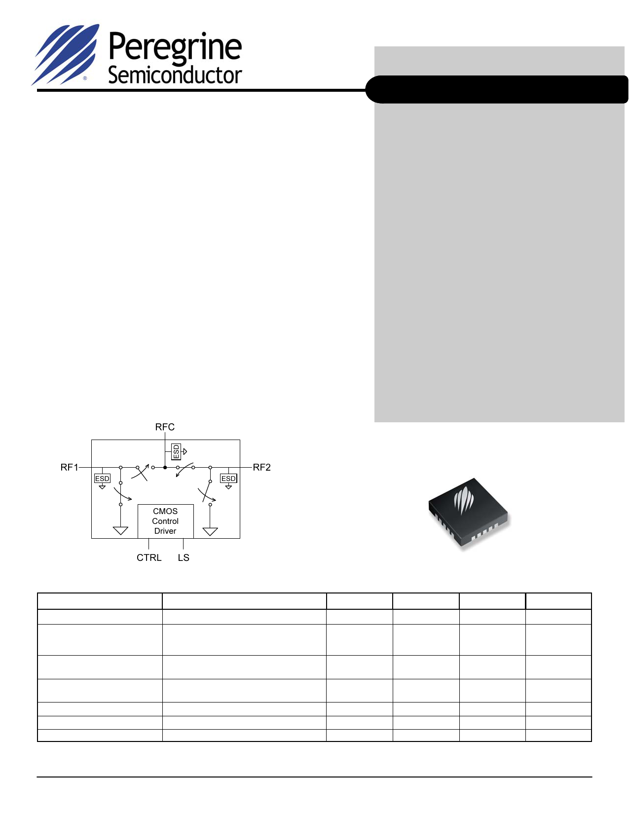
The PE42551 RF Switch is designed to support the
requirements of the test equipment and ATE market. This
broadband general purpose switch maintains excellent RF
performance and linearity from 9 kHz through 6000 MHz. The
PE42551 integrates on-board CMOS control logic driven by a
single-pin, low voltage CMOS control input. It also has a logic
select pin which enables changing the logic definition of the
control pin. Additional features include a novel user defined
logic table, enabled by the on-board CMOS circuitry. The
PE42551 also exhibits outstanding isolation that approaches
21 dB at 6000 MHz and is offered in a small 4x4x0.85 mm
QFN package.
The PE42551 is manufactured on PeregrineРђЎs UltraCMOS┬«
process, a patented variation of silicon-on-insulator (SOI)
technology on a sapphire substrate, offering the performance of
GaAs with the economy and integration of conventional CMOS.
Figure 1. Functional Diagram
Peregrine Specification 71-0065
Product Specification
PE42551
SPDT UltraCMOS® RF Switch
9 kHz - 6000 MHz
Features
Рђб HaRPРёб-Technology РђЊEnhanced
Рђб Eliminates Gate and Phase Lag
Рђб No insertion loss nor phase drift
Рђб Fast settling time
Рђб High linearity 50 dBm IIP3
Рђб Low insertion loss: 0.65 dB at 3000 MHz,
0.90 dB at 6000 MHz
Рђб High isolation of 29 dB at 3000 MHz,
21 dB at 6000 MHz
Рђб High power 1 dB compression point
of +34 dBm
Рђб ESD: 500 V HBM
Рђб Single-pin 2.75V CMOS logic control
Рђб Logic select pin to change definition of
logic control
Рђб Reflective switch design
Рђб 20-lead 4x4x0.85 mm QFN package
Figure 2. Package Type
20-lead 4x4x0.85 mm QFN
Table 1. Electrical Specifications @ +25┬░C, VDD = 2.75V (ZS = ZL = 50 Рёд)
Parameter
Conditions
Min
Operation Frequency
Insertion Loss
Isolation РђЊ RF1 to RF2
Return Loss
RF1, RF2 and RFC
Switching Time
Input 1 dB Compression
Input IP3
9 kHz
3000 MHz
6000 MHz
3000 MHz
6000 MHz
3000 MHz
6000 MHz
50% CTRL to 0.1 dB final value
6000 MHz
6000 MHz
9 kHz
28
14
32
Note: Device linearity will begin to degrade below 10 MHz.
Typical
0.55
0.65
0.90
29
21
18
14
7
34
+50
Max
6000
0.65
0.75
Units
MHz
dB
dB
dB
dB
dB
dB
dB
┬хs
dBm
dBm
Document No. 70-0350-02 Рћѓ www.psemi.com
┬Е2010-2012 Peregrine Semiconductor Corp. All rights reserved.
Page 1 of 9
Share Link: 