PI5A125 查看數據表(PDF) - Pericom Semiconductor
零件编号
产品描述 (功能)
生产厂家
PI5A125 Datasheet PDF : 6 Pages
| |||
PI5A125
11223344556677889900112233445566778899001122334455667788990011221122334455667788990011223344556677889900112233445566778899001122112233445566778899001122334455667788990011223344S5566i77n8899g00l11e2211W223344i55d6677e8899B0011a2233n44d5566w7788i99d0011t22h3344A556677n88a9900l11o22g112233S44w556677it8899c00h1122
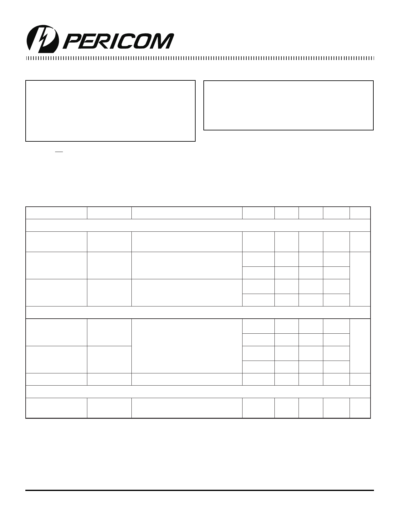
Absolute Maximum Ratings
Voltages Referenced to GND
VCC ....................................................................................... –0.5V to +7V
VOE, VA, VB(1) ................................................................ –0.5V to VCC +2V
.............................................. or 30mA, whichever occurs first
Current (any terminal except A, B) .................................. 30mA
Current: A,B (pulsed at 1ms, 10% duty cycle) .............. 120mA
Thermal Information
Continuous Power Dissipation
SOT23-5 (derate 7mW/ºC above +70ºC) ................. 550mW
Storage Temperature ................................... -65ºC to +150ºC
Lead Temperature (soldering, 10s) ........................... +300ºC
Note 1:
Signals on OE, A, B exceeding Vcc or GND are clamped by
internal diodes. Limit forward diode current to 30mA.
Caution: Stresses beyond those listed under “Absolute Maximum Ratings” may cause permanent damage to the device. This is a stress only rating
and operation of the device at these or any other conditions beyond those indicated in the operational sections of this specification is not implied.
Electrical Specifications-Single +3.3V Supply (VCC = +3.3V ± 10%, GND = 0V, VINH = 2.4V, VINL = 0.8V)
Parameter
Symbol
Conditions
Temp(°C) Min.(1) Typ.(2) Max.(1) Units
Analog Switch
Analog Signal
Range(3)
VANALOG
0
VCC
V
On-Resistance
On-Resistance
Flatness(3,5)
Dynamic
25
RON
VCC =3V, IB =-30mA, VA =1.5V
Full
RFLAT(ON)
VCC = 3.3V, IB = -30mA,
25
VA = 0.8V, 2.5V
Full
12
18
22
Ω
0.5
4
5
Turn-On Time
Turn-Off Time
Charge Injection(3)
tON
25
VCC =3.3V to VNO
Full
tOFF
or VNC = 1.5V, Fig.1
25
Full
Q
CL =1nf, VGEN = 0V, RGEN = 0V, Fig.2
25
15
25
40
ns
1.5
12
20
1.3
10
pC
Supply
ICC
Positive Supply
Current
VCC = 3.6V, Vin = 0V or VCC
All channels on or off
Full
1
µA
Notes:
1. The algebraic convention, where the most negative value is a minimum and the most positive is a maximum, is used in
this data sheet.
2. Typical values are for DESIGN AID ONLY, not guaranteed or subject to production testing.
3. Guaranteed by design
4. ∆RON = RON max - RON min
5. Flatness is defined as the difference between the maximum and minimum value of on-resistance measured.
6. Leakage parameters are 100% tested at maximum rated hot temperature and guaranteed by correlation at +25ºC.
7. Off Isolation = 20log10 VB / VA. See Figure 3.
3
PS8199D 01/12/01
Share Link: 