PI6C105H 查看數據表(PDF) - Pericom Semiconductor
零件编号
产品描述 (功能)
生产厂家
PI6C105H Datasheet PDF : 15 Pages
| |||
PI6C105 111222333444555666777888999000111222333444555666777888999000111222333444555666777888999000111222111222333444555666777888999000111222333444555666777888999000111222333444555666777888999000111222111222333444555666777888999000111222333444555666777888999000111222333444555666777888999000111222111222333444555666777888999000111222333444555666777888999000111222333444555666777888999000111222111222333444555666777888999000111222
Precision Clock Synthesizer
for Mobile PCs
Features
• Two copies of CPU clock with VDD of 2.5V ±5%
• 100 MHz or 66 MHz operation
• Six copies PCI clock (synchronous with CPU clock) 3.3V
• One copy of Ref. clock @ 14.31818 MHz (3.3VTTL)
• 48 MHz USB Clock, 24 MHz Super I/O clock
• I2C Serial Configuration Interface
• Spread Spectrum Modulation for CPUCLK, and PCICLK
• Low-cost 14.31818 MHz crystal oscillator input
• Power management control
• Isolated core VDD, VSS pins for noise reduction
• 28-pin SSOP and SOIC package (H)
Description
The PI6C105 is a high-speed, low-noise clock generator designed
to work with the PI6C18x family of clock buffers to meet all clock
needs for Mobile Intel Architecture platforms. CPU and chipset
clock frequencies of 66.6 MHz and 100 MHz are supported.
Split supplies of 3.3V and 2.5V are used. The 3.3V power supply
powers a portion of the I/O and the core. The 2.5V is used to power
the remaining outputs. 2.5V signaling follows JEDEC standard
8-X. Power sequencing of the 3.3V and 2.5V supplies is not
required.
An asynchronous PWR_DWN# signal may be used to power down
(or up) the system in an orderly manner.
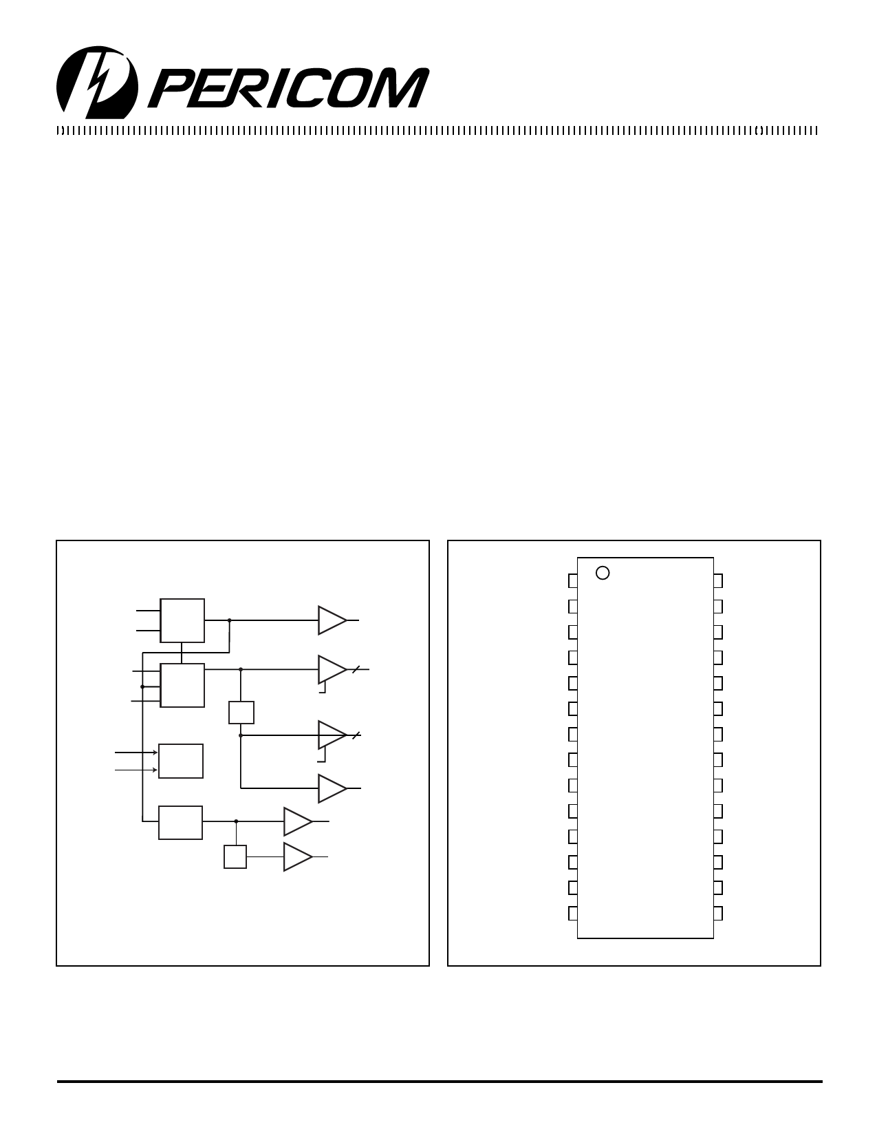
Block Diagram
Pin Configuration
XTAL_IN
XTAL_OUT
Spread#
SEL100/66#
SDATA
SCLK
REF
OSC
PLL1
I2C
PLL2
REF
CPU_STOP#
DIV
PCI_STOP#
2 CPUCLK
[0:1]
5 PCICLK
[1:5]
PCICLK_F
48 MHz
÷2
24 MHz
XTAL_IN 1
XTAL_OUT 2
VSSPCI 3
PCICLK_F 4
PCICLK1 5
PCICLK2 6
PCICLK3 7
PCICLK4 8
VDDPCI 9
PCICLK5 10
VDDP2 11
48M/SPREAD# 12
VSSP2 13
24M/SEL100/66# 14
28-Pin
H
28 VSSREF
27 VDDREF
26 REF
25 VDDCPU
24 CPUCLK0
23 CPUCLK1
22 VSSCPU
21 VDDCORE
20 VSSCORE
19 PCI_STOP#
18 CPU_STOP#
17 PWR_DWN#
16 SDATA
15 SCLK
248
PS8316 03/15/99
Share Link: 