PI6C105H 查看數據表(PDF) - Pericom Semiconductor
零件编号
产品描述 (功能)
生产厂家
PI6C105H Datasheet PDF : 15 Pages
| |||
PI6C105
111222333444555666777888999000111222333444555666777888999000111222333444555666777888999000111222111222333444555666777888999000111222333444555666777888999000111222333444555666777888999000111222111222333444555666777888999000111222333444555666777888P999000r111e222c333444is555666i777o888n999000111C222111l222o333c444555k666777S888999y000111n222t333h444555e666777s888i999z000e111r222333f444555o666r777888M999000111o222111b222i333l444e555666P777888C999000111s222
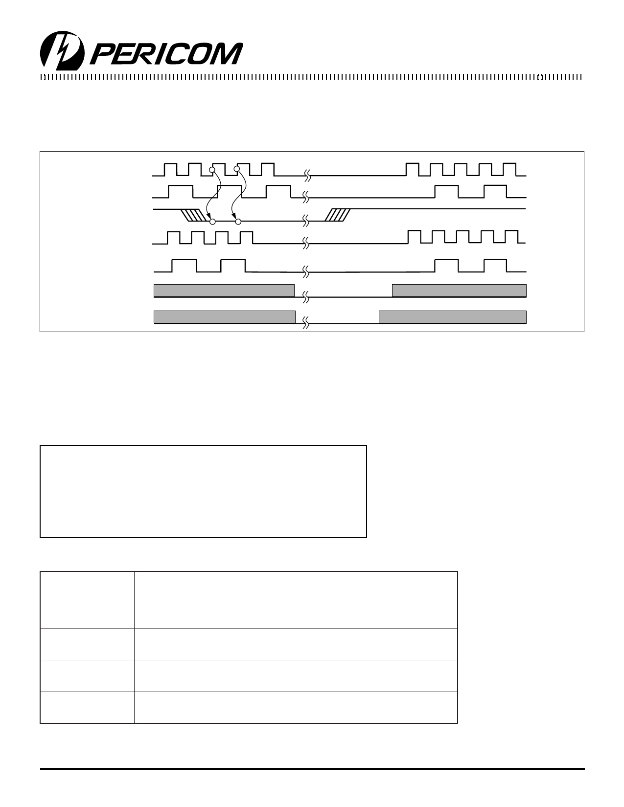
The PWR_DWN#, which is used to place the device in a very low The power on latency is less than 3ms. PCI_STOP# and
power state, is an asynchronous active low input. Internal clocks CPU_STOP# are “don’t cares” during the power down operations.
are stopped after the device is put in power down mode.
The REF clock is stopped in the LOW state as soon as possible.
CPUCLK
(Internal)
PCICLK
(Internal)
PWR_DWN#
CPUCLK
(External)
PCICLK
(External)
VCO
Crystal
Notes:
PWR_DWN# Timing Diagram
1. All timing is referenced to the CPUCLK.
2. The Internal label means inside the chip and is a reference only.
3. PWR_DWN# is an asynchronous input and metastable conditions could exist. The signal is synchronized inside the part.
4. The Shaded sections on the VCO and the Crystal signals indicate an active clock.
5. Diagrams shown wth respect to 66 MHz. Similar operations as CPU = 100 MHz.
Maximum Ratings
(Above which the useful life may be impaired. For user guidelines, not tested.)
Storage Temperature ............................................................ 65°C to +150°C
Ambient Temperature with Power Applied ............................. 0°C to +70°C
3.3V Supply Voltage to Ground Potential ............................. 0.5V to +4.6V
2.5V Supply Voltage to Ground Potential ............................. 0.5V to +3.6V
DC Input Voltage ................................................................... 0.5V to +4.6V
Note:
Stresses greater than those listed under MAXIMUM
RATINGS may cause permanent damage to the device.
This is a stress rating only and functional operation of the
device at these or any other conditions above those
indicated in the operational sections of this specification
is not implied. Exposure to absolute maximum rating
conditions for extended periods may affect reliability.
DC Electrical Characteristics (TA = 0°C to +70°C)
PI6C105
Condition
Max. 2.5V Supply Consumption
Max. discrete cap loads,
VDDCPU = 2.625V
All static inputs = VDD or VSS
Powerdown Mode
(PWRDWN# = 0)
100µA
Active 66 MHz
SEL 100/66# = 0
72mA
Active 100 MHz
SEL 100/66# = 1
100mA
Max. 3.3V Supply Consumption
Max. discrete cap loads,
VDD = 3.465V
All static inputs = VDD or VSS
500µA
170mA
170mA
255
PS8316 03/15/99
Share Link: 