PI74ALVCH162268A 查看數據表(PDF) - Pericom Semiconductor
零件编号
产品描述 (功能)
生产厂家
PI74ALVCH162268A Datasheet PDF : 6 Pages
| |||
PI74ALVCH162268
1234567890123456789012345678901212345678901234567890112234-5B67i8t90T12o1223445-6B78i9t01R23e45g6i7s8t90e1r2e34d56B78u90s12E12x34c5h67a8n90g12e3r456w78i9t0h12334-5S67t8a90t1e21O23u45t6p78u9t01s2
Maximum Ratings
(Above which the useful life may be impaired. For user guidelines, not tested.)
Storage Temperature .................................................. 65°C to +150°C
Supply Voltage Range, VCC ........................................... 0.5V to 4.6V
Input Voltage Range,VI :
Except I/O ports (See Note 1): ........................................ 0.5V to 4.6V
I/O ports (See Notes 1 and 2) .............................. 0.5V to VCC + 0.5V
Output Voltage Range, VO (See Notes 1and 2) .. 0.5V to VCC + 0.5V
Input Clamp current, IIK (VI < 0) .............................................. 50mA
Output Clamp current, IOK (VO < 0 or VO > VCC) ................... ±50mA
Continous Output Current, IO (VO = 0 to VCC) ........................ ±50mA
Continous Current through each VCC or GND ........................ ±100mA
Maximum Power Dissipation:
A package ................................................................... 1W
V package ................................................................ 1.4W
Note:
Stresses greater than those listed under MAXIMUM
RATINGS may cause permanent damage to the device.
This is a stress rating only and functional operation of the
device at these or any other conditions above those
indicated in the operational sections of this specification
is not implied. Exposure to absolute maximum rating
conditions for extended periods may affect reliability.
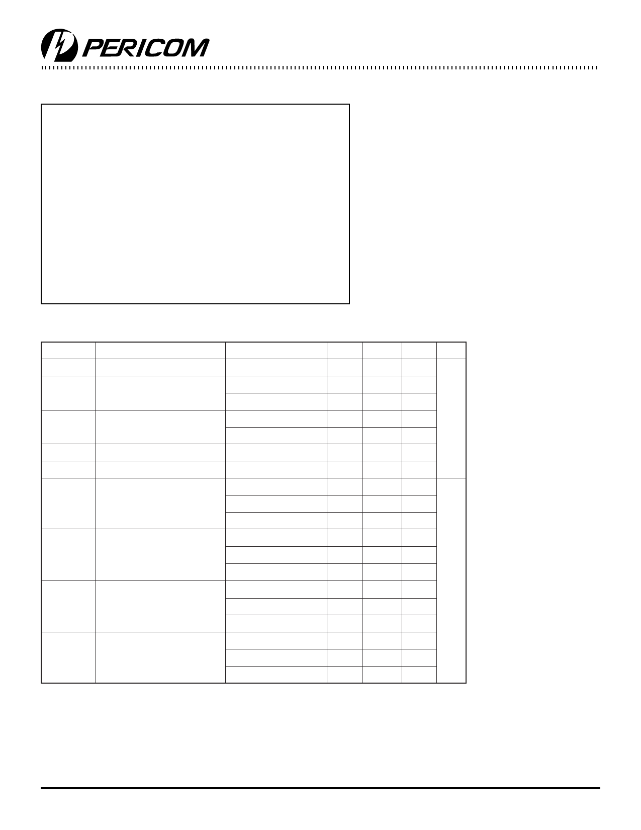
DC Electrical Characteristics (Over the Operating Range, TA = –40°C to +85°C, VCC = 3.3V ± 10%)
Parameters
Description
Test Conditions(3)
Min. Typ. Max. Units
VCC
Supply Voltage
2.3
3.6
VIH
Input HIGH Voltage
VIL
Input LOW Voltage
VIN
Input Voltage
VCC = 2.3V to 2.7V
1.7
VCC = 2.7V to 3.6V
2.0
VCC = 2.3V to 2.7V
VCC = 2.7V to 3.6V
0
0.7
V
0.8
VCC
VOUT Output Voltage
0
VCC
VCC = 2.3V
-12
IOH
HIGH-level Output Current
(A Port)
VCC = 2.7V
-12
VCC = 3.0V
-24
IOL
LOW-level Output Current
(A Port)
IOH
HIGH-level Output Current
(B Port)
VCC = 2.3V
VCC = 2.7V
VCC = 3.0V
VCC = 2.3V
VCC = 2.7V
VCC = 3.0V
12
12
24
mA
-6
-8
-12
LOW-level
VCC = 2.3V
6
IOL
Output Current
VCC = 2.7V
8
(B Port)
VCC = 3.0V
12
Notes:
1. The input and output negative-voltage ratings maybe exceeded if the input and outputclamp-current ratings are observed.
2. This value is limited to 4.6V maximum.
3. Unused control inputs must be held HIGH or LOW to prevent them from floating.
3
PS8352 11/04/98
Share Link: 