PI74FCT2646T 查看數據表(PDF) - Pericom Semiconductor
零件编号
产品描述 (功能)
生产厂家
PI74FCT2646T Datasheet PDF : 7 Pages
| |||
PI74FCT646/648/651/652T
(25Ω Series) P174FCT2646T/2652T
1234567890123456789012345678901212345678901234567890123456789012123456789012345678O90C123T45A67L890R12E12G345I6S78T90E12R34E56D789T01R234A56N78S90C12E12I3V456E78R90S12
PI74FCT646/648T
PI74FCT651/652T
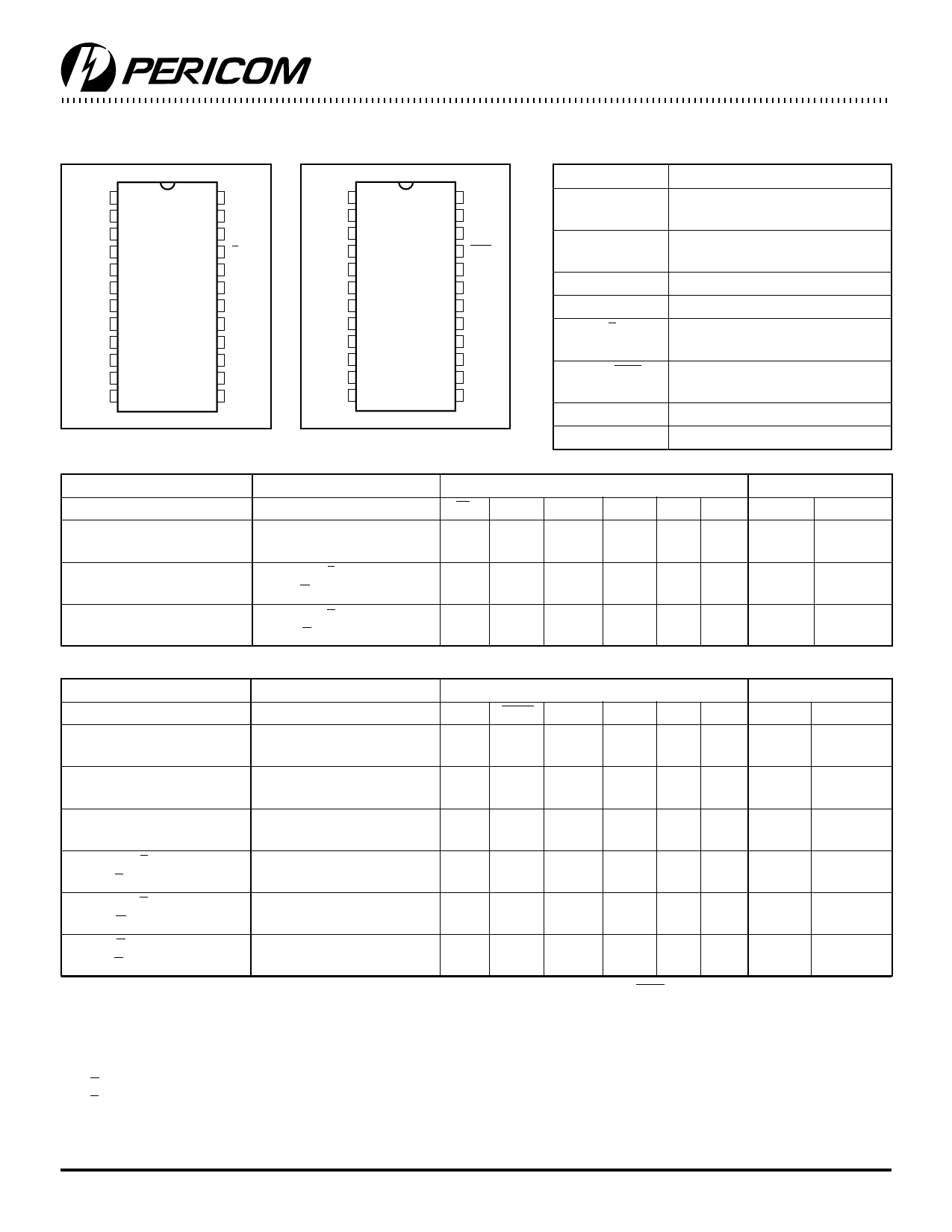
Product Pin Configuration Product Pin Configuration
CPAB
SAB
DIR
A0
A1
A2
A3
A4
A5
A6
A7
GND
1
24
2
23
3
22
4 24-PIN 21
5 P24 20
6 Q24 19
7 R24 18
8 S24 17
9
16
10
15
11
14
12
13
Vcc
CPBA
SBA
G
B0
B1
B2
B3
B4
B5
B6
B7
CPAB
SAB
GAB
A0
A1
A2
A3
A4
A5
A6
A7
GND
1
24
2
23
3
22
4 24-PIN 21
5 P24 20
6 Q24 19
7 R24 18
8 S24 17
9
16
10
15
11
14
12
13
Vcc
CPBA
SBA
GBA
B0
B1
B2
B3
B4
B5
B6
B7
PI74FCT646/648/2646T Truth Table
PI74FCT646/2646T
PI74FCT648T
Function/Operation
Function/Operation
G DIR
Isolation
Store A and B Data
Isolation
Store A and B Data
H
X
H
X
Real Time B Data to A Bus Real Time B Data to A Bus L
L
Stored B Data to A Bus Stored B Data to A Bus
L
L
Real Time A Data to B Bus Real Time A Data to B Bus L
H
Stored A Data to B Bus Stored A Data to B Bus
L
H
Product Pin Description
Pin Name
A0-A7
B0-B7
CPAB, CPBA
SAB, SBA
DIR, G
GAB, GBA
GND
VCC
Description
Data Register A Inputs
Data Register B Outputs
Data Register B Inputs
Data Register A Outputs
Clock Pulse Inputs
Output Data Source Select Inputs
Output Enable Inputs
(646/648/2646)
Output Enable Inputs
(651/652/2652)
Ground
Power
Inputs
CPAB CPBA SAB
H or L H or L X
↑
↑X
X
XX
X H or L X
X
XL
H or L X H
SBA
X
X
L
H
X
X
DATA I/O(2)
A0-A7 B0-B7
Input Input
Output Input
Input Output
PI74FCT651/652/2652T Truth Table
PI74FCT651T
PI74FCT652/2652T
Function/Operation
Function/Operation
GAB
Isolation
Isolation
L
Store A and B Data
Store A and B Data
L
Store A, Hold B
Store A, Hold B
X
Store A in Both Registers(3) Store A in Both Registers
H
Hold A, Store B
Hold A, Store B
L
Store B in Both Registers(4) Store B in Both Registers
L
Real Time B Data to A Bus Real Time B Data to A Bus L
Stored B Data to A Bus Stored B Data to A Bus
L
Real Time A Data to B Bus Real Time A Data to B Bus H
Stored A Data to B Bus Stored A Data to B Bus
H
Stored A Data to B Bus and Stored A Data to B Bus and H
Stored B Data to A Bus Stored B Data to A Bus
GBA
H
H
H
H
X
L
L
L
H
H
L
Inputs
CPAB CPBA SAB
H or L H or L X
↑
↑X
↑ H or L X
↑
↑
X(2)
H or L ↑ X
↑
↑X
X
XX
X H or L X
X
XL
H or L X H
H or L H or L H
DATA I/O(2)
SBA A0-A7 B0-B7
X Input
X
Input
X Input Unspecified(1)
X Input Output
X Unspecified(1) Input
X(2) Output Input
L Output
H
Input
X Input Output
X
H Output Output
1. The data output functions may be enabled or disabled by various signals at the GAB or GBA inputs. Data
input functions are always enabled, i.e., data at the bus pins will be stored on every low-to-high transition
on the clock inputs.
2. Select control = L: clocks can occur simultaneously.
Select control = H: clocks must be staggered in order to load both registers.
3. A in B Register
4. B in A Register
2
PS2022A 03/11/96
Share Link: 