AD9288(1999) 查看數據表(PDF) - Analog Devices
零件编号
产品描述 (功能)
生产厂家
AD9288 Datasheet PDF : 16 Pages
| |||
AD9288
to differential by transformers T1, T2—allowing the ADC perfor-
mance for differential inputs to be measured using a single-
ended source. In this mode use jumpers E1–E2, E3–E4, E7–E8
and E9–E10. (E4–E5 and E6–E7 jumpers should be lifted.)
Each analog input is terminated on the board with 50 Ω to
ground. Each input is ac-coupled on the board through a 0.1 µF
capacitor to an on-chip resistor divider that provides dc bias.
Note that the inverting analog inputs are terminated on the
board with 25 Ω (optimized for single-ended operation). When
driving the board differentially these resistors can be changed to
50 Ω to provide balanced inputs.
Encode
The encode clock for channel A uses SMB connector J7. Chan-
nel B encode is at SMB connector J2. Each clock input is termi-
nated on the board with 50 Ω to ground. The input clocks are
fed directly to the ADC and to buffers U5, U6 which drive the
DAC and latches. The clock inputs are TTL compatible, but
should be limited to a maximum of VD.
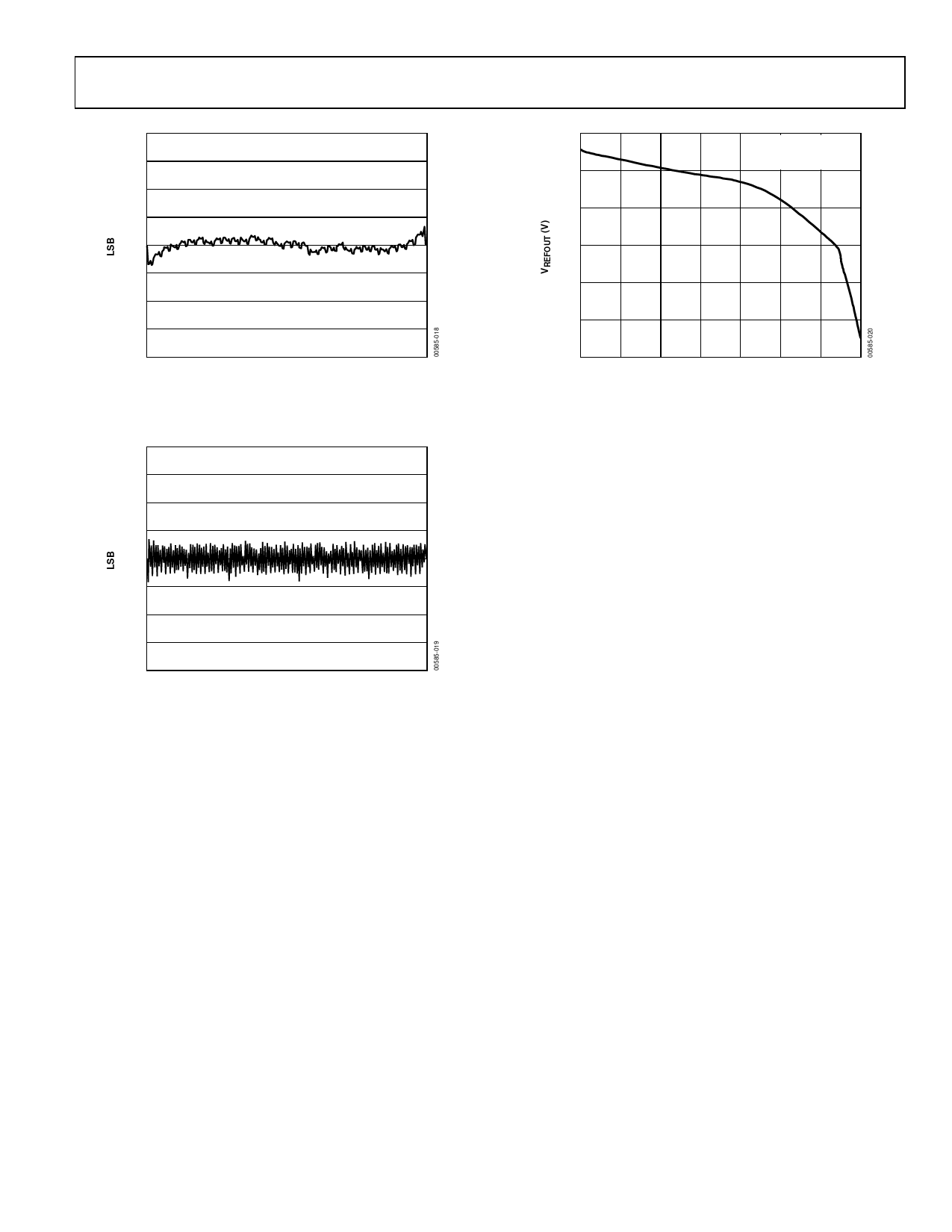
Voltage Reference
The AD9288 has an internal 1.25 V voltage reference. An ex-
ternal reference for each channel may be employed instead. The
evaluation board is configured for the internal reference (use
jumpers E18–E41 and E17–E19. To use external references,
connect to VREFA and VREFB pins on the power connector
P1 and use jumpers E20–E18 and E21–E19.
Normal Operation Mode
In this mode both converters are clocked by the same encode
clock; latency is four clock cycles (see timing diagram). Signal
S1 (Pin 8) is held high and signal S2 (Pin 9) is held low. This is
set at jumpers E22–E29 and E26–E23.
Data Align Mode
In this mode channel B output is delayed an additional 1/2 cycle.
Signal S1 (Pin 8) and signal S2 (Pin 9) are both held high. This
is set at jumpers E22–E29 and E26–E28.
Data Format Select
Data Format Select sets the output data format that the ADC
outputs. Setting DFS (Pin 4) low at E30–E27 sets the output
format to be offset binary; setting DFS high at E30–E25 sets
the output to be twos complement.
Data Outputs
The ADC digital outputs are latched on the board by two 574s,
the latch outputs are available at the 37-pin connector at Pins
22–29 (Channel A) and Pins 30–37 (Channel B). A latch out-
put clock (data ready) is available at Pin 2 or 21 on the output
connector. The data ready signal can be aligned with clock A
input by connecting E31–E32 or aligned with clock B input by
connecting E31–E33.
PIN 22 (DATA)
1
PIN 2 (CLOCK)
Ch1 2.00V CH2 2.00V M 10.0ns CH4 40mV
Figure 24. Data Output and Clock at 37-Pin Connector
DAC Outputs
Each channel is reconstructed by an on-board dual channel
DAC, an AD9763. This DAC is intended to assist in debug—it
should not be used to measure the performance of the ADC. It
is a current output DAC with on-board 50 Ω termination resis-
tors. Figure 25 is representative of the DAC output with a full-
scale analog input. The scope setting was low bandwidth, 50 Ω
termination.
1
Ch1 500mV⍀BW
M 50.0ns CH1 380mV
Figure 25. AD9763 Reconstruction DAC Output
Troubleshooting
If the board does not seem to be working correctly, try the
following:
• Verify power at IC pins.
• Check that all jumpers are in the correct position for the
desired mode of operation.
• Verify VREF is at 1.25 V
• Try running encode clock and analog inputs at low speeds
(10 MSPS/1 MHz) and monitor 574 outputs, DAC outputs,
and ADC outputs for toggling.
The AD9288 Evaluation Board is provided as a design example
for customers of Analog Devices, Inc. ADI makes no warran-
ties, express, statutory, or implied, regarding merchantability or
fitness for a particular purpose.
REV. 0
–11–
Share Link: 