LTC1196(Rev_0) 查看數據表(PDF) - Linear Technology
零件编号
产品描述 (功能)
生产厂家
LTC1196 Datasheet PDF : 28 Pages
| |||
LTC1196/LTC1198
APPLICATI S I FOR ATIO
Clock Frequency
The maximum recommended clock frequency is 14.4MHz
at 25°C for the LTC1196/LTC1198 running off a 5V supply.
With the supply voltage changing, the maximum clock
frequency for the devices also changes (see the typical
curve of Maximum Clock Rate vs Supply Voltage). If the
supply is reduced, the clock rate must be reduced also. At
3V the devices are specified with a 5.4MHz clock at 25°C.
Mixed Supplies
It is possible to have a digital system running off a 5V
supply and communicate with the LTC1196/LTC1198
operating on a 3V supply. Achieving this reduces the
outputs of DOUT from the ADCs to toggle the equivalent
input of the digital system. The CS, CLK and DIN inputs of
the ADCs will take 5V signals from the digital system
without causing any problem (see typical curve of Digital
Input Logic Threshold vs Supply Voltage). With the
LTC1196 operating on a 3V supply, the output of DOUT only
goes between 0V and 3V. This signal easily meets TTL
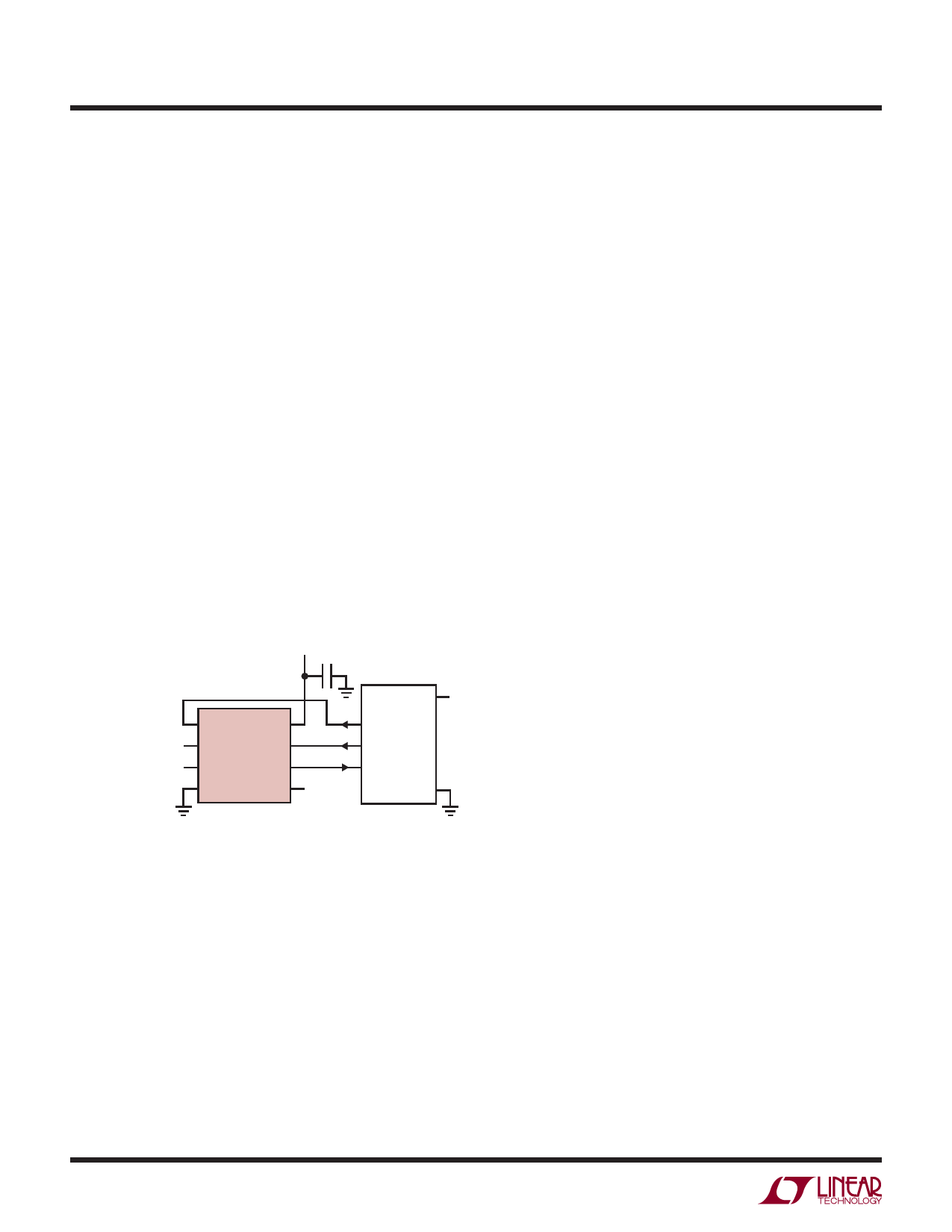
levels (see Figure 6).
3V
4.7µF
CS
VCC
DIFFERENTIAL INPUTS
COMMON-MODE RANGE
0V TO 3V
+IN
CLK
LTC1196
–IN
DOUT
GND
VREF 3V
MPU
5V
(e.g., 8051)
P1.4
P1.3
P1.2
1196/98 F06
Figure 6. Interfacing a 3V Powered LTC1196 to a 5V System
BOARD LAYOUT CONSIDERATIONS
Grounding and Bypassing
The LTC1196/LTC1198 are easy to use if some care is
taken. They should be used with an analog ground plane
and single-point grounding techniques. The GND pin
should be tied directly to the ground plane.
The VCC pin should be bypassed to the ground plane with
a 1µF tantalum with leads as short as possible. If the power
supply is clean, the LTC1196/LTC1198 can also operate
with smaller 0.1µF surface mount or ceramic bypass
capacitors. All analog inputs should be referenced directly
to the single-point ground. Digital inputs and outputs
should be shielded from and/or routed away from the
reference and analog circuitry.
SAMPLE-AND-HOLD
Both the LTC1196 and the LTC1198 provide a built-in
sample-and-hold (S&H) function to acquire the input
signal. The S&H acquires the input signal from “+” input
during tSMPL as shown in Figures 1 and 2. The S&H of the
LTC1198 can sample input signals in either single-ended
or differential mode (see Figure 7).
Single-Ended Inputs
The sample-and-hold of the LTC1198 allows conversion
of rapidly varying signals. The input voltage is sampled
during the tSMPL time as shown in Figure 7. The sampling
interval begins as the bit preceding the first DUMMY bit is
shifted in and continues until the falling CLK edge after the
second DUMMY bit is received. On this falling edge, the
S&H goes into hold mode and the conversion begins.
Differential Inputs
With differential inputs, the ADC no longer converts just a
single voltage but rather the difference between two volt-
ages. In this case, the voltage on the selected “+” input is
still sampled and held and therefore may be rapidly time
varying just as in single-ended mode. However, the volt-
age on the selected “–” input must remain constant and be
free of noise and ripple throughout the conversion time.
Otherwise, the differencing operation may not be per-
formed accurately. The conversion time is 8.5 CLK cycles.
Therefore, a change in the “–” input voltage during this
interval can cause conversion errors. For a sinusoidal
voltage on the “–” input, this error would be:
VERROR (MAX) = VPEAK × 2 × π × f(“–”) × 8.5/ fCLK
Where f(“–”) is the frequency of the “–” input voltage,
VPEAK is its peak amplitude and fCLK is the frequency of the
18
Share Link: 